background image

2-12


AC Timings  

Figure 2-5 is a graphical representation of Table 2-14.

Note:

The UPM machine and GPCM machine outputs change on the internal tick determined by the 
memory controller programming; the AC specifications are relative to the internal tick. SDRAM 
machine outputs change only on the 

REFCLK

 rising edge.

Figure 2-5. Internal Tick Spacing for Memory Controller Signals

Table 2-15.   AC Characteristics for SIU Inputs

Number

Characteristic Value

Units

10

Hold time for all signals after REFCLK rising edge

0.5

ns

11

AACK/ARTRY/TA/TEA/DBG/BG/BR setup time before REFCLK rising edge

5

ns

12

Data bus setup time before REFCLK rising edge
a. Normal mode
b. ECC and parity mode

4.55

6

ns
ns

14

DP setup time before REFCLK rising edge

6

ns

15

Setup time before REFCLK rising edge for all other signals

4

ns

Note:

Input specifications are measured from the TTL signal level (0.8 or 2.0 V) relative to the REFCLK rising 
edge.

Table 2-16.   AC Characteristics for SIU Outputs 

Number

Characteristic Maximum

Minimum

Units

31 PSDVAL/TEA/TA delay from REFCLK rising edge

9

1.0

ns

32a

Address bus/Address attributes/GBL delay from REFCLK rising 
edge

8.5

1.0

ns

32b

BADDR delay from REFCLK rising edge

10

1.0

ns

33a

Data bus delay from REFCLK rising edge

8.5

1.0

ns

33b

DP delay from REFCLK rising edge

10

1.0

ns

34

Memory controller signals/ALE delay from REFCLK rising edge

5.5

1.0

ns

35

All other signals delay from REFCLK rising edge

6

1.0

ns

Note:

Output specifications are measured from the 1.4 V level of the REFCLK rising edge to the TTL signal level 
(0.8 or 2.0 V).

REFCLK

T1

T2

T3

T4

REFCLK

T1

T2

T3

T4

for 1:2.5 

for 1:3.5 

REFCLK

T1

T2

T3

T4

for 1:2, 1:3, 1:4, 1:5, 1:6

Summary of Contents for Digital DNA MSC8101

Page 1: ... MSC8101 is offered in three core speed levels 250 275 and 300 MHz The Motorola MSC8101 DSP is a very versatile device that integrates the high performance SC140 four ALU Arithmetic Logic Unit DSP core along with 512 KB of on chip memory a Communications Processor Module CPM a 64 bit bus a very flexible System Integration Unit SIU and a 16 channel DMA engine on a single device With its four ALU co...

Page 2: ...age Information 3 1 3 2 FC PBGA Package Description 3 1 3 3 FC PBGA Package Mechanical Drawing 3 32 Chapter 4 Design Considerations 4 1 Thermal Design Considerations 4 1 4 2 Electrical Design Considerations 4 2 4 3 Power Considerations 4 2 4 4 Layout Practices 4 4 Index Ordering Information Disclaimer and Contact Information Back Cover Data Sheet Conventions OVERBAR Used to indicate a signal that ...

Page 3: ...ecutes long filters such as echo cancellation Runs at 300 MHz and provides 300 MMACS performance Programmable Memory Controller Control for up to eight banks of external memory User programmable machines UPM allowing glueless interface to various memory types SRAM DRAM EPROM and Flash memory and other user definable peripherals Dedicated pipelined SDRAM memory interface Large On Chip SRAM 256K 16 ...

Page 4: ...ature Distribution Center The World Wide Web WWW Table 1 MSC8101 Documentation Name Description Order Number MSC8101 Technical Data MSC8101 features list and physical electrical timing and package specifications MSC8101 D MSC8101 User s Guide Detailed functional description of the MSC8101 memory configuration operation and register programming MSC8101UG D MSC8101 Pocket Guide Quick reference infor...

Page 5: ...r Module CPM is a subset of the parallel I O signals supported by the MPC8260 device port pins are not numbered sequentially Table 1 1 MSC8101 Functional Signal Groupings Functional Group Number of Signal Connections Detailed Description Power VCC VDD and GND 80 Table 1 1 on page 1 4 Clock 6 Table 1 2 on page 1 5 Reset Configuration and EOnCE 11 Table 1 3 on page 1 6 System Bus HDI16 and Interrupt...

Page 6: ...BIT TRST 1 1 D60 HCS2 TDO 1 4 D 61 63 Reserved 1 Reserved DP0 Reserved EXT_Br2 EOnCE Event RESET Configuration 1 IRQ1 DP1 IRQ1 EXT_BG2 EED 1 1 IRQ2 DP2 Reserved EXT_DBG2 EE0 DBREQ 1 1 IRQ3 DP3 Reserved EXT_BR3 EE1 HPE 1 1 IRQ4 DP4 DREQ3 EXT_BG3 EE 2 3 2 1 IRQ5 DP5 DREQ4 EXT_DBG3 EE 4 5 BTM 0 1 2 1 IRQ6 DP6 DACK3 IRQ6 PORESET 1 1 IRQ7 DP7 DACK4 IRQ7 RSTCONF 1 1 TA HRESET 1 1 TEA SRESET 1 1 NMI 1 NM...

Page 7: ...1TXD3 L1TSYNC PB25 TXD2 TXD2 L1RXD3 L1RSYNC PB24 TXD1 TXD1 L1RXD2 TDMD2 L1TXD PB23 TXD0 TXD TXD0 L1RXD1 L1RXD PB22 RXD0 RXD RXD0 L1TXD2 L1TSYNC PB21 RXD1 RXD1 L1TXD1 L1RSYNC I2 C PB20 RXD2 RXD2 SDA PB19 RXD3 RXD3 SCL BRGs Clocks Timers PB18 Ext Req BRG1O CLK1 TGATE1 PC31 EXT1 BRG2O CLK2 TOUT1 PC30 SCC1 CTS CLSN BRG3O CLK3 TIN2 PC29 CTS CLSN SIU Timer Input BRG4O CLK4 TIN1 TOUT2 PC28 CLK5 BRG5O CLK...

Page 8: ...ed with an extremely low impedance path to the VCC power rail VCCSYN1 SC140 PLL Power VCC dedicated for use with the SC140 core PLL The voltage should be well regulated and the input should be provided with an extremely low impedance path to the VCC power rail GND System Ground An isolated ground for the internal processing logic This connection must be tied externally to all chip ground connectio...

Page 9: ...Output Output Clock Mode Input 2 Defines the operating mode of internal clock circuits Transfer Code 1 Supplies information that can be useful for debugging bus transactions initiated by the MSC8101 Bank Select 1 Selects the SDRAM bank when the MSC8101 is in 60x compatible bus mode MODCK3 TC2 BNKSEL2 Input Output Output Clock Mode Input 3 Defines the operating mode of internal clock circuits Trans...

Page 10: ...word EOnCE Event 1 After PORESET is deasserted you can configure EE1 as an input default or an output Enable Address Event Detection Channel 1 or generate one of the EOnCE events Debug Acknowledge or detection by Address Event Detection Channel 1 Used to trigger external debugging equipment EE21 Input Output EOnCE Event 2 After PORESET is deasserted you can configure EE2 as an input default or an ...

Page 11: ...r external debugging equipment EED1 Input Output Enhanced OnCE EOnCE Event Detection After PORESET is deasserted you can configure EED as an input default or output Enable the Data Event Detection Channel Detection by the Data Event Detection Channel Used to trigger external debugging equipment PORESET Input Power On Reset When asserted this line causes the MSC8101 to enter power on reset state RS...

Page 12: ...gner must select one line for each required interrupt and reconfigure the other external signal line or lines for alternate functions Table 1 4 System Bus HDI16 and Interrupt Signals Signal Data Flow Description A 0 31 Input Output Address Bus When the MSC8101 is in external master bus mode these pins function as the address bus The MSC8101 drives the address of its internal bus masters and respon...

Page 13: ...a service routine via the internal interrupt controller from the SC140 core BR Input Output Output Input Bus Request2 An output when an external arbiter is used The MSC8101 asserts this pin to request ownership of the bus An input when an internal arbiter is used An external master should assert this pin to request bus ownership from the internal arbiter BG Input Output Output Input Bus Grant2 An ...

Page 14: ...utput for the duration of the data bus tenure Following a TA which terminates the data bus tenure the MSC8101 deasserts DBB for a fraction of a bus cycle and then stops driving this pin The MSC8101 does not assume data bus ownership as long as it senses DBB is asserted by an external bus master Interrupt Request 31 One of the eight external lines that can request a service routine via the internal...

Page 15: ...drives the valid data on this pin Host Data Strobe3 When the HDI16 is programmed to interface with a single data strobe host bus this pin is the data strobe Schmitt trigger input HDS HDS The polarity of the data strobe is programmable Host Write Data Strobe3 When the HDI16 is programmed to interface with a double data strobe host bus this pin is the write data strobe Schmitt trigger input HWR HWR ...

Page 16: ...Bus Bit 58 In write transactions the bus master drives the valid data on this pin In read transactions the slave drives the valid data on this pin Host Dual Data Strobe3 When the HDI16 interface is enabled this pin is the host dual data strobe HDDS D59 H8BIT Input Output Input Data Bus Bit 59 In write transactions the bus master drives the valid data on this pin In read transactions the slave driv...

Page 17: ...n external bus master IRQ2 DP2 EXT_DBG2 Input Input Output Output Interrupt Request 21 One of eight external lines that can request a service routine via the internal interrupt controller from the SC140 core Data Parity 21 The agent that drives the data bus also drives the data parity signals The value driven on the data parity two pin should give odd parity odd number of ones on the group of sign...

Page 18: ... bus master IRQ6 DP6 DACK3 Input Input Output Output Interrupt Request 61 One of eight external lines that can request a service routine via the internal interrupt controller from the SC140 core Data Parity 61 The agent that drives the data bus also drives the data parity signals The value driven on the data parity six pin should give odd parity odd number of ones on the group of signals that incl...

Page 19: ... external lines that can request a service routine via the internal interrupt controller from the SC140 core Interrupt Output1 Driven from the MSC8101 internal interrupt controller Assertion of this output indicates that an unmasked interrupt is pending in the MSC8101 internal interrupt controller Notes 1 See the System Interface Unit SIU chapter in the MCS8101 Reference Manual for details on how ...

Page 20: ...er in the MS8101 Technical Reference manual for details PWE 0 7 PSDDQM 0 7 PBS 0 7 Output Output Output Bus Write Enable Outputs of the bus General Purpose Chip select Machine GPCM These pins select byte lanes for write operations Bus SDRAM DQM Outputs of the SDRAM control machine These pins select specific byte lanes of SDRAM devices Bus UPM Byte Select Outputs of the User Programmable Machine UP...

Page 21: ...TA PUPMWAIT PPBS PGPL4 Input Input Output Output GPCM TA Terminates transactions during GPCM operation Requires an external pull up resistor for proper operation Bus UPM Wait Input to the UPM An external device can hold this pin high to force the UPM to wait until the device is ready for the operation to continue Bus Parity Byte Select In systems in which data parity is stored in a separate chip t...

Page 22: ...the following protocols IEEE 802 3 Fast Ethernet through a Media Independent Interface MII HDLC Protocol Serial mode Transfers data one bit at a time Nibble mode Transfers data four bits at a time Synchronous Data Link Control SDLC LocalTalk HDLC based local area network protocol Universal Asynchronous Receiver Transmitter UART Synchronous UART 1x clock mode Binary Synchronous BISYNC communication...

Page 23: ...CRS MII Output Input Input Output Input FCC1 UTOPIA Slave Transmit Cell Available In the ATM UTOPIA interface supported by FCC1 TXCLAV is asserted by the MSC8101 UTOPIA slave PHY when the MSC8101 can accept one complete ATM cell FCC1 UTOPIA Master Transmit Cell Available In the ATM UTOPIA interface supported by FCC1 TXCLAV is asserted by an external UTOPIA slave PHY to indicate that it can accept ...

Page 24: ...C1 UTOPIA Master Receive Enable In the ATM UTOPIA interface supported by FCC1 UTOPIA slave RXENB is an input asserted by an external PHY to indicate that RXD 0 7 and RXSOC is to be sampled at the end of the next cycle RXD 0 7 and RXSOC are enabled only in cycles following those with RXENB asserted FCC1 Media Independent Interface Transmit Enable In the MII interface supported by FCC1 TX_EN is asse...

Page 25: ... on TXD 0 7 TXD7 is the most significant bit TXD0 is the least significant bit When no ATM data is available idle cells are inserted A cell is 53 bytes Module Serial Number Bit 0 MSNUM 0 4 of is the sub block code of the current peripheral controller using SDMA MSNUM5 indicates which section transmit 0 or receive 1 is active during the transfer PA24 FCC1 TXD1 UTOPIA SDMA MSNUM1 Output Output FCC1 ...

Page 26: ...ut FCC1 UTOPIA Transmit Data Bit 5 TXD 0 7 is part of the ATM UTOPIA interface supported by FCC1 The MSC8101 outputs ATM cell octets UTOPIA interface data on TXD 0 7 TXD7 is the most significant bit TXD0 is the least significant bit When no ATM data is available idle cells are inserted A cell is 53 bytes FCC1 MII and HDLC Nibble Transmit Data Bit 2 TXD 3 0 is supported by MII and HDLC nibble modes...

Page 27: ... RXD0 is the least significant bit When no ATM data is available idle cells are inserted A cell is 53 bytes To support Multi PHY configurations RXD 0 7 is tri stated enabled only when RXENB is asserted FCC1 MII and HDLC Nibble Receive Data Bit 0 RXD 3 0 is supported by MII and HDLC nibble mode in FCC1 RXD3 is the most significant bit RXD0 is the least significant bit FCC1 HDLC Serial and Transpare...

Page 28: ... HDLC nibble mode in FCC1 RXD3 is the most significant bit RXD0 is the least significant bit PA13 FCC1 RXD3 UTOPIA SDMA MSNUM2 Input Output FCC1 UTOPIA Receive Data Bit 3 In the ATM UTOPIA interface supported by FCC1 The MSC8101 inputs ATM cell octets UTOPIA interface data on RXD 0 7 RXD7 is the most significant bit RXD0 is the least significant bit A cell is 53 bytes To support Multi PHY configur...

Page 29: ...he least significant bit A cell is 53 bytes To support Multi PHY configurations RXD 0 7 is tri stated enabled only when RXENB is asserted Module Serial Number Bit 5 MSNUM 0 4 of is the sub block code of the current peripheral controller using SDMA MSNUM5 indicates which section transmit 0 or receive 1 is active during the transfer PA9 SMC2 SMTXD SI1 TDMA1 L1TXD0 TDM nibble Output Output SMC2 Seria...

Page 30: ...ta from L1RXD PA7 SMC2 SMSYN SI1 TDMA1 L1TSYNC TDM nibble and TDM serial Input Input SMC2 Serial Management Synchronization The SMC interface consists of SMTXD SMRXD SMSYN and a clock Not all signals are used for all applications SMCs are full duplex ports that supports three protocols or modes UART transparent or general circuit interface GCI Time Division Multiplexing A1 Layer 1 Transmit Synchro...

Page 31: ...put Input Input SCC2 Transmit Data Supported by SCC2 SCC2 transmits serial data out of TXD FCC2 Media Independent Interface Receive Data Valid In the MII interface supported by FCC2 RX_DV is asserted by an external fast Ethernet PHY RX_DV indicates that valid data is being sent The presence of carrier sense but not RX_DV indicates reception of broken packet headers probably due to bad wiring or a ...

Page 32: ...n Ethernet mode Time Division Multiplexing B2 Layer 1 Transmit Synchronization In the TDMB2 interface supported by SI2 this is the synchronizing signal for the transmit channel See the Serial Interface with Time Slot Assigner chapter in the MSC8101 Technical Reference manual PB27 FCC2 COL MII SI2 TDMC2 L1TXD TDM serial Input Output FCC2 Media Independent Interface Collision Detect In the MII inter...

Page 33: ...least significant bit Time Division Multiplexing A1 Nibble Layer 1 Receive Data Bit 3 TDMA1 receives nibble data into L1RXD 0 3 L1RXD3 is the most significant bit and L1RXD0 is the least significant bit in nibble mode Time Division Multiplexing C2 Layer 1 Receive Synchronization In the TDMC2 interface supported by SI2 this is the synchronizing signal for the receive channel PB23 FCC2 TXD1 MII and ...

Page 34: ... PB21 FCC2 RXD0 MII and HDLC nibble FCC2 RXD HDLC serial and transparent SI1 TDMA1 L1TXD2 TDM nibble SI2 TDMD2 L1TSYNC TDM serial Input Input Output Input FCC2 MII and HDLC Nibble Receive Data Bit 0 RXD 0 3 is supported by MII and HDLC nibble mode in FCC2 RXD3 is the most significant bit RXD0 is the least significant bit FCC2 HDLC Serial and Transparent Receive Data Supported by HDLC serial mode a...

Page 35: ... 2 RXD 0 3 is supported by MII and HDLC nibble mode in FCC2 RXD3 is the most significant bit RXD0 is the least significant bit I2 C Inter Integrated Circuit Serial Data The I2 C interface comprises two signals serial data SDA and serial clock SDA The I2C controller uses a synchronous multimaster bus that can connect several integrated circuits on a board Clock rates run up to 520 kHz 25 MHz system...

Page 36: ...by an external gate signal There are two gate signals TGATE1 controls timer 1 and or 2 and TGATE2 controls timer 3 and or 4 PC30 BRG2O CLK2 Timer1 TOUT1 EXT1 Output Input Output Input Baud Rate Generator 2 Output The CPM supports up to 8 BRGs The BRGs can be used internally by the bank of clocks selection logic and or provide an output to one of the 8 BRG pins Clock 2 The CPM supports up to 10 clo...

Page 37: ...The CPM supports up to 8 BRGs The BRGs can be used internally by the bank of clocks selection logic and or provide an output to one of the 8 BRG pins Clock 4 The CPM supports up to 10 clock input pins The clocks are sent to the bank of clocks selection logic where they can be routed to the controllers Timer Input 1 A timer can have one of the following sources another timer system clock system clo...

Page 38: ... Rate Generator 6 Output The CPM supports up to 8 BRGs The BRGs can be used internally by the bank of clocks selection logic and or provide an output to one of the 8 BRG pins Clock 6 The CPM supports up to 10 clock input pins The clocks are sent to the bank of clocks selection logic where they can be routed to the controllers Timer 3 Timer Out 3 The timers Timer 1 4 can output a signal on a timer ...

Page 39: ...he CPM supports up to 8 BRGs The BRGs can be used internally by the bank of clocks selection logic and or provide an output to one of the 8 BRG pins Clock 8 The CPM supports up to 10 clock input pins The clocks are sent to the bank of clocks selection logic where they can be routed to the controllers Timer Input 3 A timer can have one of the following sources another timer system clock system cloc...

Page 40: ...ved for future development PC22 SI1 L1ST1 CLK10 DMA DREQ1 Output Input Input Output Serial Interface 1 Layer 1 Strobe 1 In the time slot assigner supported by SI1 The MSC8101 time slot assigner supports up to four strobe outputs that can be asserted on a bit or byte basis The strobe outputs are useful for interfacing to other devices that do not support the multiplexed interface or for enabling di...

Page 41: ...IA master FCC1 RXADDR0 UTOPIA slave Output Input Output Input Serial Interface 1 Layer 1 Strobe 2 In the time slot assigner supported by SI1 The MSC8101 time slot assigner supports up to four strobe outputs that can be asserted on a bit or byte basis The strobe outputs are useful for interfacing to other devices that do not support the multiplexed interface or for enabling disabling three state I ...

Page 42: ...interface supported by FCC1 this is transmit address bit 1 PC12 SI1 L1ST3 SCC2 CD RENA FCC1 RXADDR1 UTOPIA master FCC1 RXADDR1 UTOPIA slave Output Input Output Input Serial Interface 1 Layer 1 Strobe 3 In the time slot assigner supported by SI1 The MSC8101 time slot assigner supports up to four strobe outputs that can be asserted on a bit or byte basis The strobe outputs are useful for interfacing...

Page 43: ... forms for such applications as stepper motor control FCC1 Clear To Send In the standard modem interface signals supported by FCC1 RTS CTS and CD CTS is asynchronous with the data FCC1 UTOPIA Multi PHY Master Transmit Address Bit 2 In the ATM UTOPIA master interface supported by FCC1 this is transmit address bit 2 FCC1 UTOPIA Multi PHY Slave Transmit Address Bit 2 In the ATM UTOPIA slave interface...

Page 44: ... 2 FCC1 UTOPIA Multi PHY Master Receive Cell Available 1 Direct Polling In the ATM UTOPIA master interface supported by FCC1 using direct polling RXCLAV1 is asserted by an external PHY when one complete ATM cell is available for transfer PC5 SMC1 SMTXD SI2 L1ST3 FCC2 CTS HDLC serial HDLC nibble and transparent Output Output Input SMC1 Transmit Data Supported by SMC1 The SMC interface consists of S...

Page 45: ... The MSC8101 time slot assigner supports up to four strobe outputs that can be asserted on a bit or byte basis The strobe outputs are useful for interfacing to other devices that do not support the multiplexed interface or for enabling disabling three state I O buffers in a multiple transmitter architecture These strobes can also generate output wave forms for such applications as stepper motor co...

Page 46: ...nnot be used simultaneously There are two sets of DMA pins associated with the PIO ports DMA Done 2 DACK2 DREQ2 DRACK2 and DONE2 belong to the SIU DMA DONE2 and DRACK2 are signals on the same pin and therefore cannot be used simultaneously There are two sets of DMA pins associated with the PIO ports PD29 SCC1 RTS TENA FCC1 RXADDR3 UTOPIA master FCC1 RXADDR3 UTOPIA slave FCC1 RXCLAV2 UTOPIA multi P...

Page 47: ...o one of the 8 BRG pins BRG1O can be the internal input to the SIU timers When CLK5 is selected see PC27 above it is the source for BRG1O which is the default input for the SIU timers See the System Interface Unit SIU chapter in the MSC8101 Technical Reference manual for additional information If CLK5 is not enabled BRG1O uses an internal input If TMCLK is enabled see PC26 above the BRG1O input to...

Page 48: ...BRG2O FCC1 RXPRTY UTOPIA SPI SPIMOSI Output Input Input Output Baud Rate Generator 2 Output The CPM supports up to 8 BRGs The BRGs can be used internally to the MSC8101 and or provide an output to one of the 8 BRG pins FCC1 UTOPIA Receive Parity In the ATM UTOPIA interface supported by FCC1 this is the odd parity bit for RXD 0 7 SPI Master Output Slave Input The SPI interface comprises our signals...

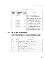
Page 49: ...1 UTOPIA Multi PHY Master Transmit Cell Available 2 Direct Polling In the ATM UTOPIA master interface supported by FCC1 using direct polling TXCLAV2 is asserted by an external UTOPIA slave PHY to indicate that it can accept one complete ATM cell Table 1 7 JTAG Test Access Port Signals Signal Name Type Signal Description TCK Input Test Clock A test clock signal for synchronizing JTAG test logic TDI...

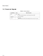
Page 50: ...ed Signals Signal Name Type Signal Description TEST Input Test Used for manufacturing testing You must connect this input to GND THERM 1 2 Leave disconnected SPARE1 5 Spare Pins Leave disconnected for backward compatibility with future revisions of this device ...

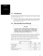
Page 51: ...on of process parameter values in one direction The minimum specification is calculated using the worst case for the same parameters in the opposite direction Therefore a maximum value for a specification never occurs in the same device with a minimum value for another specification adding a maximum to a minimum represents a condition that can never exist Table 2 1 describes the maximum electrical...

Page 52: ...ing Symbol Value Unit SC140 Core supply voltage VDD 1 5 to 1 7 V PLL supply voltage VCCSYN 1 5 to 1 7 V I O supply voltage VDDH 3 135 to 3 465 V Input voltage VIN 0 2 to VDDH 0 2 V Operating temperature range TJ 40 to 105 C Table 2 3 Thermal Characteristics Characteristic Symbol FC PBGA 17 17mm Unit Junction to ambient1 2 RθJA or θJA 52 C W Junction to ambient four layer board1 3 RθJA or θJA 25 C ...

Page 53: ...ts except CLKIN VIH 2 0 3 465 V Input low voltage VIL GND 0 8 V CLKIN input high voltage VIHC 2 5 3 465 V CLKIN input low voltage1 VILC GND 0 8 V Input leakage current VIN VDDH IIN 10 µA Tri state high impedance off state leakage current VIN VDDH IOZ 10 µA Signal low input current VIL 0 4 V IL 4 0 mA Signal high input current VIH 2 0 V IH 4 0 mA Output high voltage IOH 2 mA except open drain pins ...

Page 54: ...s deasserted Clock configuration changes only when the internal PORESET signal is deasserted The following factors are configured SPLL pre division factor SPLL PDF SPLL multiplication factor SPLL MF Bus post division factor Bus DF The SCC division factor SCC DF is fixed at 4 and the CPM division factor CPM DF is fixed at 2 The BRG division factor BRG DF is configured through the System Clock Contr...

Page 55: ...W RESET 16 17 18 19 20 21 22 23 24 25 26 27 28 29 30 31 DFBRG TYPE R W RESET Figure 2 1 System Clock Control Register SCCR 0x10C80 Table 2 7 SCCR Bit Descriptions Name Bit No Defaults Description Settings PORESET Hard Reset 0 29 Reserved DFBRG 30 31 01 Unaffected Division Factor for the BRG Clock Defines the BRGCLK frequency Changing this value does not result in a loss of lock condition 00 Divide...

Page 56: ... other combinations not used CPMDF 12 15 Configuration Pins Unaffected CPM Division Factor 0001 CPM DF 2 All other combinations are not used SPLLPDF 16 19 Configuration Pins Unaffected SPLL Pre Division Factor 0000 SPLL PDF 1 0001 SPLL PDF 2 0010 SPLL PDF 3 0011 SPLL PDF 4 All other combinations not used SPLLMF 20 23 Configuration Pins Unaffected SPLL Multiplication Factor 0110 SPLL MF 12 0111 SPL...

Page 57: ...e frequency after the predivider SPLLMFCLK higher than 18 MHz 2 CLKIN should have a 50 5 duty cycle Table 2 10 Clock Ranges Clock Symbol Maximum Rated Core Frequency All Max Values for SC140 Clock Rating of Min 250 MHz 275 MHz 300 MHz Input Clock CLKIN 18 MHz 62 5 68 75 MHz 75 MHz SPLL MF Clock SPLLMFCLK 18 MHz 20 83 22 9 MHz 25 MHz Bus BCLK 18 MHz 62 5 MHz 68 75 MHz 75 MHz Output CLKOUT 43 2 MHz ...

Page 58: ...reset configuration host reset configuration and hardware reset configuration 2 7 2 2 Power On Reset Flow Asserting the PORESET external pin initiates the power on reset flow PORESET should be asserted externally for at least 16 input clock cycles after external power to the MSC8101 reaches at least 2 3 VCC As Table 2 12 shows the MSC8101 has five configuration pins four of which are multiplexed w...

Page 59: ...ode 00 MSC8101 boots from external memory 01 MSC8101 boots from HDI16 10 Reserved 11 Reserved Table 2 13 Reset Timing No Characteristics Expression Min Max Unit 1 Required external PORESET duration minimum CLKIN 18 MHz CLKIN 75 MHz 16 CLKIN 888 8 213 3 ns ns 2 Delay from deassertion of external PORESET to deassertion of internal PORESET CLKIN 18 MHz CLKIN 75 MHz 1024 CLKIN 56 89 13 65 µs µs 3 Dela...

Page 60: ...ed if HPE is sampled low at the rising edge of PORESET The value driven on RSTCONF while PORESET changes from assertion to deassertion determines the MSC8101 configuration If RSTCONF is deasserted driven high while PORESET changes the MSC8101 acts as a configuration slave If RSTCONF is asserted driven low while PORESET changes the MSC8101 acts as a configuration master Section 2 7 2 4 Hardware Res...

Page 61: ... DLLIN or if the DLL is disabled CLKOUT Memory controller signals however trigger on four points within a REFCLK cycle Each cycle is divided by four internal ticks T1 T2 T3 and T4 T1 always occurs at the rising edge of REFCLK and T3 at the falling edge but the spacing of T2 and T4 depends on the PLL clock ratio selected as Table 2 14 shows Figure 2 4 Hardware Reset Configuration Timing Table 2 14 ...

Page 62: ...dge 6 ns 15 Setup time before REFCLK rising edge for all other signals 4 ns Note Input specifications are measured from the TTL signal level 0 8 or 2 0 V relative to the REFCLK rising edge Table 2 16 AC Characteristics for SIU Outputs Number Characteristic Maximum Minimum Units 31 PSDVAL TEA TA delay from REFCLK rising edge 9 1 0 ns 32a Address bus Address attributes GBL delay from REFCLK rising e...

Page 63: ...als REFCLK AACK ARTRY TA TEA DBG BG BR DATA bus All other inputs PSDVAL TEA TA Address bus Address attributes GBL Data bus 10 10 10 15 12 11 DP input 10 14 31 BADDR 32a 32b DP output 33a 33b Memory controller ALE 34 All other outputs 35 ...

Page 64: ...r REFCLK rising edge 0 5 ns 76 DACK DRACK DONE delay after REFCLK rising edge 0 5 9 ns Figure 2 7 DMA Signals Table 2 18 Host Interface HDI16 Timing1 2 Number Characteristics3 Expression Min Max Unit 44a Read data strobe assertion width4 HACK read assertion width TC 3 3 6 6 ns 44b Read data strobe deassertion width4 HACK read deassertion width TC 3 3 6 6 ns 44c Read data strobe deassertion width4 ...

Page 65: ... 10 2 5 TC 3 3 11 6 ns 63 Delay from DMA HACK OAD 0 or Read Write data strobe OAD 1 deassertion to HREQ assertion 2 5 TC 3 3 11 6 ns 64 Delay from DMA HACK OAD 0 or Read Write data strobe OAD 1 assertion to HREQ deassertion 3 5 TC 3 3 14 9 ns Notes 1 TC 1 DSPCLK At 300 MHz TC 3 3 ns 2 In the timing diagrams below the controls pins are drawn as active low The pin polarity is programmable 3 VCC 3 3 ...

Page 66: ... Timing Diagram Double Data Strobe HDS HA 0 3 HCS 1 2 HD 0 15 50 55 44c 44b 44a 53 52 58 57 51 49 61 56 HREQ single host request HRW 57 58 HRRQ double host request HRD HA 0 3 HCS 1 2 HD 0 15 50 55 44a 44b 44a 53 52 58 57 51 49 56 61 HREQ single host request HRRQ double host request ...

Page 67: ...Figure 2 11 Write Timing Diagram Double Data Strobe HDS HA 0 3 HCS 1 2 HD 0 15 47 46 45 54 58 57 56 HRW 57 58 48 62 HREQ single host request HTRQ double host request HWR HA 0 3 HCS 1 2 HD 0 15 47 46 45 54 48 58 57 56 62 HREQ single host request HTRQ double host request ...

Page 68: ...e timing Figure 2 12 Host DMA Read Timing Diagram Figure 2 13 Host DMA Write Timing Diagram RX 0 3 Read Data Valid 64 44a 63 44b 51 50 49 52 Output HREQ HACK or HWR HDS HRD Input HD 0 15 Output TX 0 3 Write Data Valid 63 64 46 45 47 48 Output HREQ HACK or HWR HDS HRD Input HD 0 15 Output ...

Page 69: ...t hold time after low to high serial transition 20 ns 22 PIO TIMER DMA input setup time before low to high serial clock transition 10 ns 23 PIO TIMER DMA input hold time after low to high serial clock transition 3 ns Note FCC SCC SMC SPI I2 C are Non Multiplexed Serial Interface signals Table 2 20 CPM Output Characteristics No Characteristic Min Max Unit 36 FCC output delay after low to high clock...

Page 70: ... TDM Signal Diagram Figure 2 19 PIO Timer and DMA Signal Diagram Serial input clock FCC inputs FCC outputs 16b 17b 36b BRGxO SCC SMC SPI I2C inputs SCC SMC SPI I2C outputs 18a 19a 38a Serial input clock SCC SMC SPI I2C inputs SCC SMCSPI I2C outputs 18b 19b 38b Serial input clock TDM inputs TDM outputs 20 21 40 REFCLK PIO TIMER DMA inputs PIO TIMER DMA outputs 22 23 42 ...

Page 71: ...ics Type Minimum 65 EE pins as inputs Asynchronous 4 DSPCLKs 66 EE pins as outputs Synchronous to DSPCLK 1 DSPCLK Notes 1 DSPCLK is the SC140 core clock The ratio between DSPCLK and CLKOUT is configured during power on reset See AN2288 for details 2 Direction of the EE pins is configured in the EE_CTRL register of the EOnCE See the SC140 Core Reference Manual MNSC140DSPCORERM D 3 Refer to Table 1 ...

Page 72: ...Test Access Port Timing Diagram Figure 2 23 TRST Timing Diagram TCK Input VM VM VIH VIL 501 502 502 503 503 TCK Input TDI Input TDO Output TDO Output TDO Output VIH VIL Input Data Valid Output Data Valid Output Data Valid TMS 508 509 510 511 510 TCK Input TRST Input 513 512 ...

Page 73: ... 2 show top and bottom views of the FC PBGA package including pinouts Table 3 1 lists the MSC8101 signals alphabetically by signal name Connections with multiple names are listed individually by each name Signals with programmable polarity are shown both as signals which are asserted low default and high i e NAME NAME Table 3 2 lists the signals numerically by pin number Each pin number is listed ...

Page 74: ...28 A23 A19 A16 A9 A7 A11 D27 D24 D25 D26 D23 GND VDD GND GND VDDH PA12 PD7 PA9 PA10 D32 D29 D30 D31 GND D28 VDDH PC6 PC4 VDDH PC7 PA7 PC5 PA8 D37 D34 D35 D36 D33 GND VDDH TSIZ3 GND VDD PA6 ABB INT SPARE D42 D39 D40 D41 GND D38 VDD TT1 GND VDDH AACK BG ARTRY D46 D43 TA GND D44 D45 PSD BADDR GND VDDH CS6 A21 TT0 GND VDD TS TBST D51 D48 GND PWE2 D49 D50 GND BADDR PSD D47 GND A26 A1 GND VDDH A3 TT3 TT...

Page 75: ...5 A28 A23 A19 A16 A9 A7 A11 D27 D24 D25 D26 D23 GND VDD GND GND VDDH PA12 PD7 PA9 PA10 D32 D29 D30 D31 GND D28 VDDH PC6 PC4 VDDH PC7 PA7 PC5 PA8 D37 D34 D35 D36 D33 GND VDDH GND VDD PA6 ABB INT SPARE D42 D39 D40 D41 GND D38 VDD TT1 GND VDDH AACK BG ARTRY D46 D43 TA GND D44 D45 PSD BADDR GND VDDH CS6 A21 TT0 GND VDD TS TBST D51 D48 GND PWE2 D49 D50 GND BADDR PSD D47 GND A26 A1 GND VDDH A3 TT3 TT4 T...

Page 76: ... Signal Name Number A0 W15 A1 N14 A2 V15 A3 T14 A4 U15 A5 W16 A6 V16 A7 W17 A8 U16 A9 V17 A10 W18 A11 U17 A12 T16 A13 V18 A14 V19 A15 R16 A16 T17 A17 U18 A18 U19 A19 R17 A20 T18 A21 M13 A22 T19 A23 P17 A24 R18 A25 R19 A26 M14 A27 P18 A28 N17 A29 P19 A30 N18 A31 N19 AACK T12 ...

Page 77: ...19 BCTL1 L19 BG V12 BNKSEL0 E18 BNKSEL1 F18 BNKSEL2 G18 BR H17 BRG1O H3 BRG1O V2 BRG2O J3 BRG2O N7 BRG3O K3 BRG4O L3 BRG5O L7 BRG6O M2 BRG7O N1 BRG8O P1 BTM0 E1 BTM1 F3 CD for FCC1 N10 CD for FCC2 P10 CD RENA for SCC1 T6 CD RENA for SCC2 V4 CLK1 H3 CLK2 J3 Table 3 1 MSC8101 Signal Listing By Name Continued Signal Name Number ...

Page 78: ...1 COL for FCC2 M1 CRS for FCC1 J7 CRS for FCC2 M3 CS0 M16 CS1 L17 CS2 K19 CS3 L18 CS4 M19 CS5 M17 CS6 L13 CS7 M18 CTS for FCC1 T10 CTS for FCC2 W10 CTS CLSN for SCC1 K3 CTS CLSN for SCC1 V3 CTS CLSN for SCC2 L3 CTS CLSN for SCC2 T5 D0 B3 D1 A3 D2 C4 D3 B4 D4 A4 Table 3 1 MSC8101 Signal Listing By Name Continued Signal Name Number ...

Page 79: ... D11 A6 D12 G7 D13 E7 D14 D7 D15 C7 D16 B7 D17 A7 D18 F8 D19 D8 D20 C8 D21 B8 D22 A8 D23 G9 D24 D9 D25 C9 D26 B9 D27 A9 D28 F10 D29 D10 D30 C10 D31 B10 D32 A10 D33 G11 D34 D11 D35 C11 D36 B11 D37 A11 Table 3 1 MSC8101 Signal Listing By Name Continued Signal Name Number ...

Page 80: ...C13 D45 B13 D46 A13 D47 E14 D48 D14 D49 C14 D50 B14 D51 A14 D52 D15 D53 C15 D54 B15 D55 A15 D56 E16 D57 D16 D58 C16 D59 B16 D60 A16 D61 C17 D62 A17 D63 A18 DACK1 N5 DACK2 N1 DACK3 D5 DACK4 F6 DBB C18 DBG B18 DBREQ D2 Table 3 1 MSC8101 Signal Listing By Name Continued Signal Name Number ...

Page 81: ...6 DRACK1 DONE1 H2 DRACK2 DONE2 J2 DREQ1 R1 DREQ2 P1 DREQ3 C3 DREQ4 A2 EE0 D2 EE1 D1 EE2 E3 EE3 E2 EE4 E1 EE5 F3 EED F2 EXT_BG2 B1 EXT_BG3 C3 EXT_BR2 C2 EXT_BR3 B2 EXT_DBG2 D4 EXT_DBG3 A2 EXT1 H3 EXT2 N5 GBL D18 GND F11 GND F13 Table 3 1 MSC8101 Signal Listing By Name Continued Signal Name Number ...

Page 82: ...G12 GND G14 GND G6 GND G8 GND H15 GND H5 GND H7 GND J14 GND J5 GND J6 GND K13 GND K15 GND K6 GND K7 GND L14 GND L15 GND L5 GND L6 GND M15 GND M5 GND N6 GND N9 GND P11 GND P12 GND P13 GND P14 GND P15 GND P6 Table 3 1 MSC8101 Signal Listing By Name Continued Signal Name Number ...

Page 83: ... HA3 A14 HACK HACK E16 HCS1 HCS1 D15 HCS2 HCS2 A16 HD0 A10 HD1 G11 HD2 D11 HD3 C11 HD4 B11 HD5 A11 HD6 F12 HD7 D12 HD8 C12 HD9 B12 HD10 A12 HD11 D13 HD12 C13 HD13 B13 HD14 A13 HD15 E14 HDDS C16 HDS HDS B15 HDSP D16 HPE D1 HRD HRD C15 Table 3 1 MSC8101 Signal Listing By Name Continued Signal Name Number ...

Page 84: ... D5 IRQ7 F6 IRQ7 W11 L1RSYNC for SI1 TDMA1 T11 L1RSYNC for SI2 TDMB2 K4 L1RSYNC for SI2 TDMC2 P3 L1RSYNC for SI2 TDMD2 P5 L1RXD for SI1 TDMA1 Serial U10 L1RXD for SI2 TDMB2 H1 L1RXD for SI2 TDMC2 M3 L1RXD for SI2 TDMD2 T2 L1RXD0 for SI1 TDMA1 Nibble U10 L1RXD1 for SI1 TDMA1 Nibble T2 L1RXD2 for SI1 TDMA1 Nibble V1 L1RXD3 for SI1 TDMA1 Nibble P3 Table 3 1 MSC8101 Signal Listing By Name Continued Si...

Page 85: ...1 TDMA1 Nibble W9 L1TXD1 for SI1 TDMA1 Nibble P5 L1TXD2 for SI1 TDMA1 Nibble T1 L1TXD3 for SI1 TDMA1 Nibble N3 LIST1 for SI1 R1 LIST1 for SI2 T10 LIST2 for SI1 T6 LIST2 for SI2 N10 LIST3 for SI1 V4 LIST3 for SI2 W10 LIST4 for SI1 T5 LIST4 for SI2 P10 MODCK1 E18 MODCK2 F18 MODCK3 G18 MSNUM0 N2 MSNUM1 P2 MSNUM2 U8 MSNUM3 T9 MSNUM4 V8 MSNUM5 U9 NMI U5 NMI_OUT V5 PA6 T11 PA7 V10 Table 3 1 MSC8101 Sign...

Page 86: ...14 W8 PA15 W3 PA16 M7 PA17 T4 PA18 W2 PA19 R5 PA20 T3 PA21 U1 PA22 R3 PA23 P4 PA24 P2 PA25 N2 PA26 M6 PA27 L1 PA28 K1 PA29 J1 PA30 J7 PA31 G1 PB18 R4 PB19 U2 PB20 P5 PB21 T1 PB22 T2 PB23 V1 PB24 P3 PB25 N3 PB26 M3 Table 3 1 MSC8101 Signal Listing By Name Continued Signal Name Number ...

Page 87: ... K17 PBS2 K14 PBS3 J19 PBS4 H19 PBS5 D17 PBS6 B17 PBS7 F17 PC4 P10 PC5 W10 PC6 N10 PC7 T10 PC12 V4 PC13 T5 PC14 T6 PC15 V3 PC22 R1 PC23 N5 PC24 P1 PC25 N1 PC26 M2 PC27 L7 PC28 L3 PC29 K3 PC30 J3 PC31 H3 PD7 V9 PD16 U4 Table 3 1 MSC8101 Signal Listing By Name Continued Signal Name Number ...

Page 88: ...9 PGPL4 J18 PGPL5 J17 PGTA J18 POE G19 PORESET W5 PPBS J18 PSDA10 E17 PSDAMUX J17 PSDCAS E19 PSDDQM0 K18 PSDDQM1 K17 PSDDQM2 K14 PSDDQM3 J19 PSDDQM4 H19 PSDDQM5 D17 PSDDQM6 B17 PSDDQM7 F17 PSDRAS G19 PSDVAL G13 PSDWE F14 PUPMWAIT J18 PWE0 K18 PWE1 K17 Table 3 1 MSC8101 Signal Listing By Name Continued Signal Name Number ...

Page 89: ...r FCC1 M1 RX_DV for FCC2 H1 RX_ER for FCC1 M3 RX_ER for FCC2 L2 RXADDR0 for FCC1 UTOPIA 8 T6 RXADDR1 for FCC1 UTOPIA 8 V4 RXADDR2 for FCC1 UTOPIA 8 N10 RXADDR2 RXCLAV1 for FCC1 UTOPIA 8 N10 RXADDR3 for FCC1 UTOPIA 8 K2 RXADDR4 for FCC1 UTOPIA 8 U3 RXCLAV for FCC1 UTOPIA 8 M3 RXCLAV0 for FCC1 UTOPIA 8 M3 RXCLAV2 for FCC1 UTOPIA 8 K2 RXCLAV3 for FCC1 UTOPIA 8 V4 RXD for FCC1 transparent HDLC serial ...

Page 90: ...TOPIA 8 T9 RXD2 for FCC2 MII HDLC nibble U2 RXD3 for FCC1 MII HDLC nibble W8 RXD3 for FCC1 UTOPIA 8 U8 RXD3 for FCC2 MII HDLC nibble R4 RXD4 for FCC1 UTOPIA 8 W8 RXD5 for FCC1 UTOPIA 8 W3 RXD6 for FCC1 UTOPIA 8 M7 RXD7 for FCC1 UTOPIA 8 T4 RXENB for FCC1 K1 RXPRTY for FCC1 UTOPIA 8 N7 RXSOC for FCC1 M1 SCL R4 SDA U2 SMRXD for SMC1 P10 SMRXD for SMC2 U10 SMSYN for SMC1 V9 SMSYN for SMC2 V10 SMTXD f...

Page 91: ...TC0 E18 TC1 F18 TC2 G18 TCK G4 TDI H6 TDO F1 TEA G17 TEST W6 TGATE1 H3 TGATE2 L7 THERM1 C1 THERM2 D3 TIN1 TOUT2 L3 TIN2 K3 TIN3 TOUT4 P1 TIN4 N1 TMCLK M2 TMS G2 TOUT1 J3 TOUT3 M2 TRST G3 TS T13 TSIZ0 V13 TSIZ1 W13 TSIZ2 W12 TSIZ3 N11 Table 3 1 MSC8101 Signal Listing By Name Continued Signal Name Number ...

Page 92: ...AV0 for FCC1 UTOPIA 8 J7 TXCLAV1 for FCC1 UTOPIA 8 T10 TXCLAV2 for FCC1 UTOPIA 8 V9 TXCLAV3 for FCC1 UTOPIA 8 V2 TXD for FCC1 transparent HDLC serial W2 TXD for FCC2 transparent HDLC serial T2 TXD for SCC1 J2 TXD for SCC2 H1 TXD0 for FCC1 MII HDLC nibble W2 TXD0 for FCC1 UTOPIA 8 N2 TXD0 for FCC2 MII HDLC nibble T2 TXD1 for FCC1 MII HDLC nibble R5 TXD1 for FCC1 UTOPIA 8 P2 TXD1 for FCC2 MII HDLC n...

Page 93: ... T3 TXD6 for FCC1 UTOPIA 8 R5 TXD7 for FCC1 UTOPIA 8 W2 TXENB for FCC1 G1 TXPRTY for FCC1 UTOPIA 8 U4 TXSOC for FCC1 J1 VCCSYN W7 VCCSYN1 T7 VDD E12 VDD E5 VDD E9 VDD F16 VDD F4 VDD H16 VDD J4 VDD L16 VDD L4 VDD N4 VDD P16 VDD R11 VDD R13 VDD R8 VDDH E10 VDDH E11 VDDH E13 VDDH E15 VDDH E4 VDDH E6 VDDH E8 Table 3 1 MSC8101 Signal Listing By Name Continued Signal Name Number ...

Page 94: ...DH R12 VDDH R14 VDDH R15 VDDH R6 VDDH R7 VDDH R9 VDDH T15 Table 3 2 MSC8101 Signal Listing by Pin Designator Number Signal Name A2 IRQ5 DP5 DREQ4 EXT_DBG3 A3 D1 A4 D4 A5 D7 A6 D11 A7 D17 A8 D22 A9 D27 A10 D32 HD0 A11 D37 HD5 A12 D42 HD10 A13 D46 HD14 A14 D51 HA3 Table 3 1 MSC8101 Signal Listing By Name Continued Signal Name Number ...

Page 95: ...26 B10 D31 B11 D36 HD4 B12 D41 HD9 B13 D45 HD13 B14 D50 HA2 B15 D54 HDS HWR B16 D59 H8BIT B17 PWE6 PSDDQM6 PBS6 B18 DBG B19 BADDR28 C1 THERM1 C2 Reserved DP0 EXT_BR2 C3 IRQ4 DP4 DREQ3 EXT_BG3 C4 D2 C5 D5 C6 D9 C7 D15 C8 D20 C9 D25 C10 D30 C11 D35 HD3 C12 D40 HD8 C13 D44 HD12 C14 D49 HA1 C15 D53 HRW HRD Table 3 2 MSC8101 Signal Listing by Pin Designator Continued Number Signal Name ...

Page 96: ...D8 D7 D14 D8 D19 D9 D24 D10 D29 D11 D34 HD2 D12 D39 HD7 D13 D43 HD11 D14 D48 HA0 D15 D52 HCS1 D16 D57 HDSP D17 PWE5 PSDDQM5 PBS5 D18 IRQ1 GBL D19 BADDR27 E1 BTM0 EE4 E2 EE3 E3 EE2 E4 VDDH E5 VDD E6 VDDH E7 D13 E8 VDDH E9 VDD E10 VDDH E11 VDDH E12 VDD E13 VDDH E14 D47 HD15 E15 VDDH Table 3 2 MSC8101 Signal Listing by Pin Designator Continued Number Signal Name ...

Page 97: ...D F8 D18 F9 GND F10 D28 F11 GND F12 D38 HD6 F13 GND F14 PSDWE PGPL1 F15 GND F16 VDD F17 PWE7 PSDDQM7 PBS7 F18 MODCK2 TC1 BNKSEL1 F19 BCTL0 G1 PA31 FCC1 UTOPIA8 TXENB FCC1 MII COL G2 TMS G3 TRST G4 TCK G5 VDDH G6 GND G7 D12 G8 GND G9 D23 G10 GND G11 D33 HD1 G12 GND G13 PSDVAL G14 GND G15 VDDH Table 3 2 MSC8101 Signal Listing by Pin Designator Continued Number Signal Name ...

Page 98: ...C1 UTOPIA8 TXSOC FCC1 MII TX_ER J2 PD30 SCC1 TXD DMA DRACK2 DONE2 J3 PC30 EXT1 BRG2O CLK2 TOUT1 J4 VDD J5 GND J6 GND J7 PA30 FCC1 UTOPIA8 TXCLAV FCC1 UTOPIA8 TXCLAV0 FCC1 MII CRS FCC1 HDLC and transparent RTS J13 TA J14 GND J15 VDDH J16 VDDH J17 PSDAMUX PGPL5 J18 PGTA PUPMWAIT PPBS PGPL4 J19 PWE3 PSDDQM3 PBS3 K1 PA28 FCC1 UTOPIA8 RXENB FCC1 MII TX_EN K2 PD29 FCC1 UTOPIA8 RXADDR3 FCC1 UTOPIA8 RXCLA...

Page 99: ...4O CLK4 TIN1 TOUT2 L4 VDD L5 GND L6 GND L7 PC27 CLK5 BRG5O TGATE2 L13 CS6 L14 GND L15 GND L16 VDD L17 CS1 L18 CS3 L19 BCTL1 M1 PB27 FCC2 MII COL TDMC2 L1TXD M2 PC26 TMCLK BRG6O CLK6 TOUT3 M3 PB26 FCC2 MII CRS TDMC2 L1RXD M4 VDDH M5 GND M6 PA26 FCC1 UTOPIA8 RXCLAV FCC1 UTOPIA8 RXCLAV0 FCC1 MII RX_ER M7 PA16 FCC1 UTOPIA8 RXD6 FCC1 MII and HDLC nibble RXD1 M13 A21 M14 A26 M15 GND M16 CS0 M17 CS5 M18 ...

Page 100: ...R2 RXCLAV1 FCC1 CD SI2 LIST2 N11 TSIZ3 N12 TT1 N13 TT0 N14 A1 N15 VDDH N16 VDDH N17 A28 N18 A30 N19 A31 P1 PC24 DMA DREQ2 BRG8O CLK8 TIN3 TOUT4 P2 PA24 FCC1 UTOPIA8 TXD1 SDMA MSNUM1 P3 PB24 FCC2 MII and HDLC nibble TXD3 TDMA1 nibble L1RXD3 TDMC2 L1RSYNC P4 PA23 FCC1 UTOPIA8 TXD2 P5 PB20 FCC2 MII and HDLC nibble RXD1 TDMA1 nibble L1TXD1 TDMD2 L1RSYNC P6 GND P7 GND P8 DLLIN P9 GND P10 PC4 FCC2 CD SM...

Page 101: ...A1 nibble L1TXD2 TDMD2 L1TSYNC T2 PB22 FCC2 MII and HDLC nibble TXD0 FCC2 transparent and HDLC serial TXD TDMA1 nibble L1RXD1 TDMD2 L1RXD T3 PA20 FCC1 UTOPIA8 TXD5 FCC1 MII and HDLC nibble TXD2 T4 PA17 FCC1 UTOPIA8 RXD7 FCC1 MII and HDLC nibble RXD0 FCC1 transparent and HDLC serial RXD T5 PC13 FCC1 UTOPIA8 TXADDR1 SCC2 CTS CLSN SI1 LIST4 T6 PC14 FCC1 UTOPIA8 RXADDR0 SCC1 CD RENA SI1 LIST2 T7 VCCSY...

Page 102: ...MSNUM5 U10 PA8 SMC2 SMRXD TDMA1 serial L1RXD TDMA1 nibble L1RXD0 U11 SPARE5 U12 ARTRY U13 TBST U14 TT2 U15 A4 U16 A8 U17 A11 U18 A17 U19 A18 V1 PB23 FCC2 MII and HDLC nibble TXD1 TDMA1 nibble L1RXD2 TDMD2 L1TXD V2 PD19 FCC1 UTOPIA8 TXADDR4 FCC1 UTOPIA TXCLAV3 SPI SPISEL BRG1O V3 PC15 FCC1 UTOPIA8 TXADDR0 SCC1 CTS CLSN SMC2 SMTXD V4 PC12 FCC1 UTOPIA8 RXADDR1 SCC2 CD RENA SI1 LIST3 V5 NMI_OUT V6 HRE...

Page 103: ...d HDLC serial TXD W3 PA15 FCC1 UTOPIA8 RXD5 FCC1 MII and HDLC nibble RXD2 W4 SRESET W5 PORESET W6 TEST W7 VCCSYN W8 PA14 FCC1 UTOPIA8 RXD4 FCC1 MII and HDLC nibble RXD3 W9 PA9 SMC2 SMTXD TDMA1 serial L1TXD TDMA1 nibble L1TXD0 W10 PC5 FCC2 CTS SMC1 SMTXD SI2 LIST3 W11 IRQ7 INT_OUT W12 TSIZ2 W13 TSIZ1 W14 TT4 W15 A0 W16 A5 W17 A7 W18 A10 Table 3 2 MSC8101 Signal Listing by Pin Designator Continued N...

Page 104: ... D D1 D2 10 35 10 55 e E E1 14 40 REF E2 9 30 9 50 Notes 1 Dimensions and tolerancing per ASME Y14 5 1994 2 Dimensions in millimeters 3 Dimension b is the maximum solder ball diameter measured parallel to Datum A 4 PrimaryDatumA andthe seating plane are defined by the spherical crowns of the solder balls CASE 1169 01 17 00 BSC 0 80 BSC 14 40 REF 17 00 BSC 0 80 0 92 0 90 1 10 0 30 0 50 2 60 ...

Page 105: ...nt temperature C θJA package thermal resistance junction to ambient C W PD PINT PI O in W PINT IDD VDD in W chip internal power PI O power dissipation on output pins in W user determined The user should set TA and PD such that TJ does not exceed the maximum operating conditions In case TJ is too high the user should either lower the ambient temperature or the power dissipation of the chip ...

Page 106: ...1 6 V the bootstrap diodes will be reverse biased with negligible leakage current The VF should be effective at the current levels required by the processor Do not use diodes with a nominal VF that drops too low at high current 4 3 Power Considerations The internal power dissipation consists of three components PINT PCORE PSIU PCPM The power dissipation depends on the operating frequency of the di...

Page 107: ...ication operates at VDDH 3 3 V Since the address pins switch once at every second cycle the address pins frequency is a quarter of the bus frequency that is 25 MHz For the same reason the data pins frequency is 3 125 MHz Calculating internal power PCORE 200 PCORE PLCO 300 200 PLCO 250 3 300 200 3 168 PSIU 50 PSIU PLSI 100 50 PLSI 70 2 100 50 2 36 PCPM 100 PCPM PLCP 150 100 PLCP 210 6 150 100 6 142...

Page 108: ...apacitances due to the PCB traces Attention to proper PCB layout and bypassing becomes especially critical in systems with higher capacitive loads because these loads create higher transient currents in the VCC VDD and GND circuits Pull up all unused inputs or signals that will be inputs during reset Special care should be taken to minimize the noise levels on the PLL supply pins There are 2 pairs...

Page 109: ...lect CS0 7 1 16 clock 1 5 JTAG 2 23 operation 2 8 clocks System Clock Control Register SCCR 2 5 System Clock Mode Register SCMR 2 5 Communications Processor Module CPM iii coprocessor iii CPM inputs 2 20 D Data Bus 1 11 Data Bus Bit 32 47 signals 1 10 Data Bus Bit 48 51 signals 1 10 Data Bus Bit 52 signal 1 11 Data Bus Bit 53 signal 1 11 Data Bus Bit 54 signal 1 11 Data Bus Bit 55 signal 1 11 Data...

Page 110: ...r coprocessor iii frequencies maximum 2 4 functional signal groups 1 1 G Global signal 1 8 GPCM TA signal 1 17 H H8BIT H8BIT 1 12 HDI08 timing 2 15 HID16 iii Host Acknowledge HACK 1 12 Host Address Line 0 signal 1 10 Host Chip Select signal 1 11 Host Data signal 1 10 Host Data Strobe HDS 1 11 Host Data Strobe Polarity HDSP 1 12 Host Dual Data Strobe HDDS 1 12 host interface iii Host Interface timi...

Page 111: ...m reset configuration word via the Host port 2 10 reset causes 2 8 reset sources 2 8 RSTCONF 2 11 soft reset 2 9 RSTCONF 1 7 S SC140 core iii SCC SMC SPI I2C external clock diagram 2 21 SCC SMC SPI I2C internal clock diagram 2 21 SDRAM DQM PSDDQM 0 7 1 16 signal groupings 1 1 signals 1 1 EE 2 22 external 1 2 JTAG 2 22 memory controller tick spacing 2 12 multiplexed 1 1 signals external Address Ack...

Page 112: ...RQ2 1 9 1 13 Interrupt Request 3 IRQ3 1 9 1 10 1 13 Interrupt Request 4 IRQ4 1 14 Interrupt Request 5 IRQ5 1 9 1 14 Interrupt Request 6 IRQ6 1 14 Interrupt Request 7 IRQ7 1 14 1 15 Spare Pins SPARE1 5 1 46 signals external Bus UPM Wait PUPMWAIT 1 17 SIU inputs 2 13 SIU outputs 2 13 Spare Pins signal 1 46 SPLL MF 2 4 SPLL multiplication factor 2 4 SPLL PDF 2 4 SRAM iii SRESET 1 7 storage temperatur...

Page 113: ......

Page 114: ......

Page 115: ......

Page 116: ...be validated for each customer application by customer s technical experts Motorola does not convey any license under its patent rights nor the rights of others Motorola products are not designed intended or authorized for use as components in systems intended for surgical implant into the body or other applications intended to support or sustain life or for any other application in which the fail...

Reviews: