Programming Model
MOTOROLA
System Control
8-5
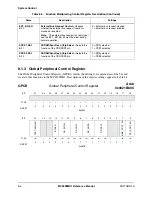
Table 8-4. Global Peripheral Control Register Description
Name
Description
Settings
Reserved
Bits 31–16
Reserved—These bits are reserved and should read 0.
TEST_EN_REG
Bit 15
Test Enable Register
- Active high of this bit switches
the internal test signals from MEMC to GPIO for
debug purposes.
0 = Normal
1 = Switches MEMC inner test
signals to GPIO for debug
purposes.
Reserved
Bits 14–13
Reserved—These bits are reserved and should read 0.
BTAEN
Bit 12
BTA Clock Input Control
—Controls the clock input
signals to the BTA module. When the bit is clear,
clock inputs to the BTA are stopped for power saving.
When this bit is set, clock inputs to the BTA are
enabled.
0 = Clock inputs to BTA disabled
1 = Clock inputs to BTA enabled
DS_SLOW
Bits 11–10
Driving Strength Slow I/O
—Controls the driving
strength of all slow I/O signals.
00 = 26 MHz/15 pF
01 = 26 MHz/30 pF
10 = 26 MHz/45 pF
11 = 26 MHz/greater than 45 pF
DS_CNTL
Bits 9–8
Driving Strength Bus Control Signal
—Controls the
driving strength of bus control signals.
00 = 50 MHz/15 pF
01 = 50 MHz/30 pF
10 = 100 MHz/15 pF
11 = 100 MHz/30 pF
DS_ADDR
Bits 7–6
Driving Strength Address Bus
—Controls the driving
strength of the address bus.
00 = 50 MHz/15 pF
01 = 50 MHz/30 pF
10 = 100 MHz/15 pF
11 = 100 MHz/30 pF
DS_DATA
Bits 5–4
Driving Strength Data Bus
—Controls the driving
strength of the data bus.
00 = 50 MHz/15 pF
01 = 50 MHz/30 pF
10 = 100 MHz/15 pF
11 = 100 MHz/30 pF
Reserved
Bit 3
Reserved—This bit must be set to 1 at all times for normal operation.
Reserved
Bit 2
Reserved—This bit is reserved and should read 0.
MMA_PROT_EN
Bit 1
MMA Privileged Mode Access
—Selects whether the
MMA can only be accessed in privileged mode or if it
can be accessed in all modes.
0 = All access modes available
1 = Privileged mode access only
CSI_PROT_EN
Bit 0
CMOS Sensor Interface Privileged Mode
Access
—Selects whether the CSI can only be
accessed in privileged mode or if it can be accessed
in all modes.
0 = All access modes available
1 = Privileged mode access only
Summary of Contents for DragonBall MC9328MX1
Page 68: ...1 12 MC9328MX1 Reference Manual MOTOROLA Introduction ...
Page 86: ...2 18 MC9328MX1 Reference Manual MOTOROLA Signal Descriptions and Pin Assignments ...
Page 116: ...3 30 MC9328MX1 Reference Manual MOTOROLA Memory Map ...
Page 126: ...4 10 MC9328MX1 Reference Manual MOTOROLA ARM920T Processor ...
Page 160: ...8 8 MC9328MX1 Reference Manual MOTOROLA System Control ...
Page 272: ...13 32 MC9328MX1 Reference Manual MOTOROLA DMA Controller ...
Page 281: ...Programming Model MOTOROLA Watchdog Timer Module 14 9 ...
Page 282: ...14 10 MC9328MX1 Reference Manual MOTOROLA Watchdog Timer Module ...
Page 300: ...15 18 MC9328MX1 Reference Manual MOTOROLA Analog Signal Processor ASP ...
Page 438: ...18 16 MC9328MX1 Reference Manual MOTOROLA Serial Peripheral Interface Modules SPI 1 and SPI 2 ...
Page 478: ...19 40 MC9328MX1 Reference Manual MOTOROLA LCD Controller ...
Page 574: ...21 32 MC9328MX1 Reference Manual MOTOROLA Memory Stick Host Controller MSHC Module ...
Page 598: ...23 16 MC9328MX1 Reference Manual MOTOROLA Real Time Clock RTC ...
Page 670: ...24 72 MC9328MX1 Reference Manual MOTOROLA SDRAM Memory Controller ...
Page 726: ...25 56 MC9328MX1 Reference Manual MOTOROLA SmartCard Interface Module SIM ...
Page 736: ...26 10 MC9328MX1 Reference Manual MOTOROLA General Purpose Timers ...
Page 854: ...29 18 MC9328MX1 Reference Manual MOTOROLA I2C Module ...
Page 900: ...30 46 MC9328MX1 Reference Manual MOTOROLA Synchronous Serial Interface SSI ...
Page 942: ...32 26 MC9328MX1 Reference Manual MOTOROLA GPIO Module and I O Multiplexer IOMUX ...


