Programming Model
MOTOROLA
DMA Controller
13-27
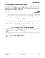
13.4.3.7 Channel Request Time-Out Registers
The channel request time-out registers (RTOx) set the time-out for DMA_REQ from the selected request
source of the channel, which detects any discontinuity of data transfer. The request time-out takes effect
only when the corresponding request enable (REN) bit in the channel control register (CCR) is set. An
internal counter starts counting when a DMA channel is enabled, the burst is completed, and the counter is
reset to zero when a DMA request is detected. When the counter reaches the count value set in the register,
it asserts an interrupt and sets its error bit in the DMA request time-out status register. The input clock of
the counter is selectable from either the system clock (HCLK) or input crystal (CLK32K).
NOTE:
This register shares the same address as the bus utilization control register.
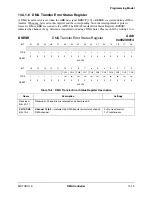
BL
Bits 5–0
Burst Length
—Contains the number of data bytes
that are transferred in a DMA burst.
000000 = 64 bytes read follow 64 bytes write
000001 = 1byte read follow 1 byte write
000010 = 2 bytes read follow 2 bytes write
....
111111 = 63 bytes read follow 63 bytes write
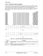
RTOR0
RTOR1
RTOR2
RTOR3
RTOR4
RTOR5
RTOR6
RTOR7
RTOR8
RTOR9
RTOR10
Channel 0 Request Time-Out Register
Channel 1 Request Time-Out Register
Channel 2 Request Time-Out Register
Channel 3 Request Time-Out Register
Channel 4 Request Time-Out Register
Channel 5 Request Time-Out Register
Channel 6 Request Time-Out Register
Channel 7 Request Time-Out Register
Channel 8 Request Time-Out Register
Channel 9 Request Time-Out Register
Channel 10 Request Time-Out Register
Addr
0x00209098
0x002090D8
0x00209118
0x00209158
0x00209198
0x002091D8
0x00209218
0x00209258
0x00209298
0x002092D8
0x00209318
BIT
31
30
29
28
27
26
25
24
23
22
21
20
19
18
17
16
TYPE
r
r
r
r
r
r
r
r
r
r
r
r
r
r
r
r
RESET
0
0
0
0
0
0
0
0
0
0
0
0
0
0
0
0
0x0000
BIT
15
14
13
12
11
10
9
8
7
6
5
4
3
2
1
0
EN
CLK
PSC
CNT
TYPE
rw
rw
rw
rw
rw
rw
rw
rw
rw
rw
rw
rw
rw
rw
rw
rw
RESET
0
0
0
0
0
0
0
0
0
0
0
0
0
0
0
0
0x0000
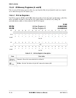
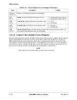
Table 13-20. Channel Burst Length Registers Description (Continued)
Name
Description
Settings
Summary of Contents for DragonBall MC9328MX1
Page 68: ...1 12 MC9328MX1 Reference Manual MOTOROLA Introduction ...
Page 86: ...2 18 MC9328MX1 Reference Manual MOTOROLA Signal Descriptions and Pin Assignments ...
Page 116: ...3 30 MC9328MX1 Reference Manual MOTOROLA Memory Map ...
Page 126: ...4 10 MC9328MX1 Reference Manual MOTOROLA ARM920T Processor ...
Page 160: ...8 8 MC9328MX1 Reference Manual MOTOROLA System Control ...
Page 272: ...13 32 MC9328MX1 Reference Manual MOTOROLA DMA Controller ...
Page 281: ...Programming Model MOTOROLA Watchdog Timer Module 14 9 ...
Page 282: ...14 10 MC9328MX1 Reference Manual MOTOROLA Watchdog Timer Module ...
Page 300: ...15 18 MC9328MX1 Reference Manual MOTOROLA Analog Signal Processor ASP ...
Page 438: ...18 16 MC9328MX1 Reference Manual MOTOROLA Serial Peripheral Interface Modules SPI 1 and SPI 2 ...
Page 478: ...19 40 MC9328MX1 Reference Manual MOTOROLA LCD Controller ...
Page 574: ...21 32 MC9328MX1 Reference Manual MOTOROLA Memory Stick Host Controller MSHC Module ...
Page 598: ...23 16 MC9328MX1 Reference Manual MOTOROLA Real Time Clock RTC ...
Page 670: ...24 72 MC9328MX1 Reference Manual MOTOROLA SDRAM Memory Controller ...
Page 726: ...25 56 MC9328MX1 Reference Manual MOTOROLA SmartCard Interface Module SIM ...
Page 736: ...26 10 MC9328MX1 Reference Manual MOTOROLA General Purpose Timers ...
Page 854: ...29 18 MC9328MX1 Reference Manual MOTOROLA I2C Module ...
Page 900: ...30 46 MC9328MX1 Reference Manual MOTOROLA Synchronous Serial Interface SSI ...
Page 942: ...32 26 MC9328MX1 Reference Manual MOTOROLA GPIO Module and I O Multiplexer IOMUX ...

