16-50
MC9328MX1 Reference Manual
MOTOROLA
Bluetooth Accelerator (BTA)
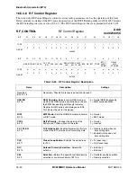
16.5.4.8 RF Control Register
The write-only RF Control Register controls various radio parameters such as the operation of the Joint
Detect module, tri-stating of the BT2 pin, and operation of the RSSI. Reading address 0x0021605C returns
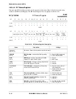
the RF Status Register (see section 16.5.4.9). The RF Control Register bits are explained in Table 16-35.
RF_CONTROL
RF Control Register
Addr
0x0021605C
BIT
31
30
29
28
27
26
25
24
23
22
21
20
19
18
17
16
TYPE
r
r
r
r
r
r
r
r
r
r
r
r
r
r
r
r
RESET
0
0
0
0
0
0
0
0
0
0
0
0
0
0
0
0
0x0000
BIT
15
14
13
12
11
10
9
8
7
6
5
4
3
2
1
0
RSSIOR BIST XPOL
TX_TRI
_EN
CLE DIV SEL
PEAK
_HLD
RSSI
_EN
PWM_
TX_EN
BT5_OE BT1_CONT
BT11_
AUTO_
SPIKE
DELAY
_HOP
_STROBE
TYPE
w
w
w
w
w
w
w
w
w
w
w
w
w
w
w
w
RESET
0
0
0
1
0
0
0
0
0
0
0
0
0
1
0
1
0x1005
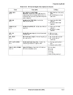
Table 16-35. RF Control Register Description
Name
Description
Settings
Reserved
Bits 31–16
Reserved—These bits are reserved and should read 0.
RSSIOR
Bit 15
RSSI Override
—Selects normal RSSI mode, or
whether the RSSI value is controlled by writing to
the PWM Received Signal Strength Indicator
Register (ARM Control) and displayed on BT8.
This bit must be set for this device.
0 = Normal RSSI functionality
1 = ARM controlled PWM
BIST
Bit 14
BIST Mode
—Sets the JD/MLSE module in normal
or BIST mode.
0 = Normal
1 = BIST mode
XPOL
Bit 13
Rx/Tx Polarity
—Changes the polarity of the
RxData and TxData signals to the radio.
0 = Normal
1 = Inverted
TX_TRI_EN
Bit 12
Tri-State Enable
—Enables/Disables the tri-state
mode of the BT2 pin when not transmitting data.
0 = Disable tri-state when not
transmitting data
1 = Enable tri-state when not
transmitting data
CLE
Bit 11
Closed Loop Enable
—Enables the closed loop
for PLL.
0 = Tx (open loop)
1 = Rx (closed loop)
DIV
Bit 10
Antenna Diversity Selection
—Selects the
antenna.
0 = Antenna 0
1 = Antenna 1
SEL
Bit 9
Selection
—Selects the operation (either diversity
selection or oscillator enable) of BT7 pin.
0 = Oscillator enable operation
1 = Diversity selection
Summary of Contents for DragonBall MC9328MX1
Page 68: ...1 12 MC9328MX1 Reference Manual MOTOROLA Introduction ...
Page 86: ...2 18 MC9328MX1 Reference Manual MOTOROLA Signal Descriptions and Pin Assignments ...
Page 116: ...3 30 MC9328MX1 Reference Manual MOTOROLA Memory Map ...
Page 126: ...4 10 MC9328MX1 Reference Manual MOTOROLA ARM920T Processor ...
Page 160: ...8 8 MC9328MX1 Reference Manual MOTOROLA System Control ...
Page 272: ...13 32 MC9328MX1 Reference Manual MOTOROLA DMA Controller ...
Page 281: ...Programming Model MOTOROLA Watchdog Timer Module 14 9 ...
Page 282: ...14 10 MC9328MX1 Reference Manual MOTOROLA Watchdog Timer Module ...
Page 300: ...15 18 MC9328MX1 Reference Manual MOTOROLA Analog Signal Processor ASP ...
Page 438: ...18 16 MC9328MX1 Reference Manual MOTOROLA Serial Peripheral Interface Modules SPI 1 and SPI 2 ...
Page 478: ...19 40 MC9328MX1 Reference Manual MOTOROLA LCD Controller ...
Page 574: ...21 32 MC9328MX1 Reference Manual MOTOROLA Memory Stick Host Controller MSHC Module ...
Page 598: ...23 16 MC9328MX1 Reference Manual MOTOROLA Real Time Clock RTC ...
Page 670: ...24 72 MC9328MX1 Reference Manual MOTOROLA SDRAM Memory Controller ...
Page 726: ...25 56 MC9328MX1 Reference Manual MOTOROLA SmartCard Interface Module SIM ...
Page 736: ...26 10 MC9328MX1 Reference Manual MOTOROLA General Purpose Timers ...
Page 854: ...29 18 MC9328MX1 Reference Manual MOTOROLA I2C Module ...
Page 900: ...30 46 MC9328MX1 Reference Manual MOTOROLA Synchronous Serial Interface SSI ...
Page 942: ...32 26 MC9328MX1 Reference Manual MOTOROLA GPIO Module and I O Multiplexer IOMUX ...

