MMA Operation
MOTOROLA
Multimedia Accelerator (MMA)
17-3
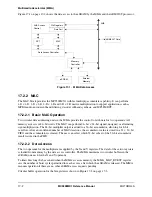
Figure 17-2. Circular Buffering Operation
17.2.2.3 Cache
The X operand access has an associated cache and cache controller. Initially, the cache is cleared and the X
operand data is accessed from the eSRAM and stored in the cache. Subsequent accesses to the same
address cause a cache hit and the data is accessed from the cache.
The cache is a memory block of 512 24–bit words. Each word also has an associated valid bit to indicate
data validity. The cache can be enabled or disabled. To fully use the cache, the base address of the operand
must be on a 2K boundary. When a data access matches an address in the cache and the valid bit for that
word is set, data is fetched from the cache. When the valid bit is cleared, data is accessed from the eSRAM
or from external memory and stored in the cache, and the valid bit is set. The cache is cleared only by
writing 1 to the CACHE CLR bit. This action also registers the base address of the 2K boundary as the
valid cache block address. The user must program the MMA_MAC_XBASE register and the
MMA_MAC_XINDEX register before clearing the cache.
eSRAM
Base Register
Points to the start
address of the circular
buffer.
Index Register
Address Index added to the
Base Register to yield the
actual physical location
a) Initially
b) After every
MMA_MAC_XCOUNT
iteration if the
X INDEX LOAD bit is set.
+
Modify Register
This value is added to the
Address Index after each
access.
+
Address Index
INDEX_LOAD
+
Increment Register
This value is added to the
Index Register after every
XCOUNT iteration if the
X INDEX INCR bit is set.
Length Register
Determines the size of the circular buffer. Actual
Index = (index - length). Actual physical location
is (Actual Index + Base)
Length
Base register added
to Index register to
produce Address
Index
Summary of Contents for DragonBall MC9328MX1
Page 68: ...1 12 MC9328MX1 Reference Manual MOTOROLA Introduction ...
Page 86: ...2 18 MC9328MX1 Reference Manual MOTOROLA Signal Descriptions and Pin Assignments ...
Page 116: ...3 30 MC9328MX1 Reference Manual MOTOROLA Memory Map ...
Page 126: ...4 10 MC9328MX1 Reference Manual MOTOROLA ARM920T Processor ...
Page 160: ...8 8 MC9328MX1 Reference Manual MOTOROLA System Control ...
Page 272: ...13 32 MC9328MX1 Reference Manual MOTOROLA DMA Controller ...
Page 281: ...Programming Model MOTOROLA Watchdog Timer Module 14 9 ...
Page 282: ...14 10 MC9328MX1 Reference Manual MOTOROLA Watchdog Timer Module ...
Page 300: ...15 18 MC9328MX1 Reference Manual MOTOROLA Analog Signal Processor ASP ...
Page 438: ...18 16 MC9328MX1 Reference Manual MOTOROLA Serial Peripheral Interface Modules SPI 1 and SPI 2 ...
Page 478: ...19 40 MC9328MX1 Reference Manual MOTOROLA LCD Controller ...
Page 574: ...21 32 MC9328MX1 Reference Manual MOTOROLA Memory Stick Host Controller MSHC Module ...
Page 598: ...23 16 MC9328MX1 Reference Manual MOTOROLA Real Time Clock RTC ...
Page 670: ...24 72 MC9328MX1 Reference Manual MOTOROLA SDRAM Memory Controller ...
Page 726: ...25 56 MC9328MX1 Reference Manual MOTOROLA SmartCard Interface Module SIM ...
Page 736: ...26 10 MC9328MX1 Reference Manual MOTOROLA General Purpose Timers ...
Page 854: ...29 18 MC9328MX1 Reference Manual MOTOROLA I2C Module ...
Page 900: ...30 46 MC9328MX1 Reference Manual MOTOROLA Synchronous Serial Interface SSI ...
Page 942: ...32 26 MC9328MX1 Reference Manual MOTOROLA GPIO Module and I O Multiplexer IOMUX ...

