LCDC Operation
MOTOROLA
LCD Controller
19-11
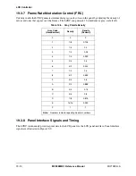
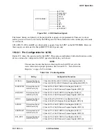
Figure 19-9. LCDC Interface Signals
The format, timing, and polarity of the panel interface signals are programmable. There are two basic
modes, passive and active, selected by the TFT register bit. The user must also select either grayscale mode
or color mode.
SPL_SPR, PS, CLS and REV are other interface signals from the LCDC on the MC9328MX1. However,
these signals are dedicated for Sharp HR-TFT 320x240 panels only.
19.3.8.1 Pin Configuration for LCDC
Figure 19-9 shows the signals used for the LCDC. These pins are multiplexed with other functions on the
device, and must be configured for LCDC operation before they can be used.
NOTE:
The user must ensure that the data direction bits in the GPIO are set to the
correct direction for proper operation. See Section 32.5.1, “Data Direction
Registers,” on page 32-9 for details.
Table 19-6. Pin Configuration
Pin
Setting
Configuration Procedure
LD [15:0]
Primary function of
GPIO Port D [30:15]
1. Clear bits [30:15] of Port D GPIO In Use Register (GIUS_D)
2. Clear bits [30:15] of Port D General Purpose Register (GPR_D)
FLM/VSYNC
Primary function of
GPIO Port D [14]
1. Clear bit 14 of Port D GPIO In Use Register (GIUS_D)
2. Clear bit 14 of Port D General Purpose Register (GPR_D)
LP/HSYNC
Primary function of
GPIO Port D [13]
1. Clear bit 13 of Port D GPIO In Use Register (GIUS_D)
2. Clear bit 13 of Port D General Purpose Register (GPR_D)
LSCLK
Primary function of
GPIO Port D [6]
1. Clear bit 6 of Port D GPIO In Use Register (GIUS_D)
2. Clear bit 6 of Port D General Purpose Register (GPR_D)
ACD/OE
Primary function of
GPIO Port D [12]
1. Clear bit 12 of Port D GPIO In Use Register (GIUS_D)
2. Clear bit 12 of Port D General Purpose Register (GPR_D)
CONTRAST
Primary function of
GPIO Port D [11]
1. Clear bit 11 of Port D GPIO In Use Register (GIUS_D)
2. Clear bit 11 of Port D General Purpose Register (GPR_D)
SPL_SPR
Primary function of
GPIO Port D [10]
1. Clear bit 10 of Port D GPIO In Use Register (GIUS_D)
2. Clear bit 10 of Port D General Purpose Register (GPR_D)
LD [15:0]
FLM/VSYNC
LP/HSYNC
LSCLK
ACD/OE
PS
CLS
REV
SPL_SPR
CONTRAST
LCD Controller
Summary of Contents for DragonBall MC9328MX1
Page 68: ...1 12 MC9328MX1 Reference Manual MOTOROLA Introduction ...
Page 86: ...2 18 MC9328MX1 Reference Manual MOTOROLA Signal Descriptions and Pin Assignments ...
Page 116: ...3 30 MC9328MX1 Reference Manual MOTOROLA Memory Map ...
Page 126: ...4 10 MC9328MX1 Reference Manual MOTOROLA ARM920T Processor ...
Page 160: ...8 8 MC9328MX1 Reference Manual MOTOROLA System Control ...
Page 272: ...13 32 MC9328MX1 Reference Manual MOTOROLA DMA Controller ...
Page 281: ...Programming Model MOTOROLA Watchdog Timer Module 14 9 ...
Page 282: ...14 10 MC9328MX1 Reference Manual MOTOROLA Watchdog Timer Module ...
Page 300: ...15 18 MC9328MX1 Reference Manual MOTOROLA Analog Signal Processor ASP ...
Page 438: ...18 16 MC9328MX1 Reference Manual MOTOROLA Serial Peripheral Interface Modules SPI 1 and SPI 2 ...
Page 478: ...19 40 MC9328MX1 Reference Manual MOTOROLA LCD Controller ...
Page 574: ...21 32 MC9328MX1 Reference Manual MOTOROLA Memory Stick Host Controller MSHC Module ...
Page 598: ...23 16 MC9328MX1 Reference Manual MOTOROLA Real Time Clock RTC ...
Page 670: ...24 72 MC9328MX1 Reference Manual MOTOROLA SDRAM Memory Controller ...
Page 726: ...25 56 MC9328MX1 Reference Manual MOTOROLA SmartCard Interface Module SIM ...
Page 736: ...26 10 MC9328MX1 Reference Manual MOTOROLA General Purpose Timers ...
Page 854: ...29 18 MC9328MX1 Reference Manual MOTOROLA I2C Module ...
Page 900: ...30 46 MC9328MX1 Reference Manual MOTOROLA Synchronous Serial Interface SSI ...
Page 942: ...32 26 MC9328MX1 Reference Manual MOTOROLA GPIO Module and I O Multiplexer IOMUX ...


