19-12
MC9328MX1 Reference Manual
MOTOROLA
LCD Controller
19.3.8.2 Passive Matrix Panel Interface Signals
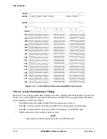
Figure 19-10 shows the LCD interface timing for monochrome panels and Figure 19-11 shows the LCD
interface timing for passive matrix color panels. Signal polarities are shown positive, however it can be
reversed by clearing the bits in the Panel Configuration Register (PCR). The data bus timing for passive
panels is controlled by the shift clock (LSCLK), line pulse (LP), first line marker (FLM), alternate crystal
direction (ACD), and line data (LD) signals. Operation of the panel interface is accomplished in the
following steps:
1. LSCLK clocks the pixel data into the display driver’s internal shift register.
2. LP signifies the end of the current line of serial data and latches the shifted pixel data into
a wide latch.
3. FLM marks the first line of the displayed page. The LD (and the associated LP), enclosed
by the FLM signal, marks the first line of the current frame.
4. ACD toggles after a pre-programmed number of FLM pulses. This signal refreshes the
LCD panel.
NOTE:
The LD bus width is programmable to 1, 2, 4, or 8 bits in monochrome
mode (the COLOR bit in the Panel Configuration register is set to 0). Data
is justified to the least significant bits of the LD [15:0] bus. Passive color
displays use a fixed 2-2/3 pixels of data per 8-bit vector as shown in
Figure 19-11.
Figure 19-10. LCDC Interface Timing for 4-bit Data Width Gray-Scale Panels
PS
Primary function of
GPIO Port D [9]
1. Clear bit 9 of Port D GPIO In Use Register (GIUS_D)
2. Clear bit 9 of Port D General Purpose Register (GPR_D)
CLS
Primary function of
GPIO Port D [8]
1. Clear bit 8 of Port D GPIO In Use Register (GIUS_D)
2. Clear bit 8 of Port D General Purpose Register (GPR_D)
REV
Primary function of
GPIO Port D [7]
1. Clear bit 7 of Port D GPIO In Use Register (GIUS_D)
2. Clear bit 7 of Port D General Purpose Register (GPR_D)
Table 19-6. Pin Configuration (Continued)
Pin
Setting
Configuration Procedure
LD0
[0,0]
[0,4]
[0,8]
LD1
[0,1]
[0,5]
[0,9]
LD2
[0,2]
[0,6]
[0,10]
LD3
[0,3]
[0,7]
[0,11]
[0,m-8]
[0,m-4]
[0,m-7]
[0,m-3]
[0,m-6]
[0,m-2]
[0,m-5]
[0,m-1]
[0,232]
[0,236]
[0,233]
[0,237]
[0,234]
[0,238]
[0,235]
[0,239]
LSCLK
1
2
3
m/4
m/4-1
59
60
LP
FLM
LP
LINE 1
LINE 2
LINE 3
LINE 4
LINE n
LINE 1
Summary of Contents for DragonBall MC9328MX1
Page 68: ...1 12 MC9328MX1 Reference Manual MOTOROLA Introduction ...
Page 86: ...2 18 MC9328MX1 Reference Manual MOTOROLA Signal Descriptions and Pin Assignments ...
Page 116: ...3 30 MC9328MX1 Reference Manual MOTOROLA Memory Map ...
Page 126: ...4 10 MC9328MX1 Reference Manual MOTOROLA ARM920T Processor ...
Page 160: ...8 8 MC9328MX1 Reference Manual MOTOROLA System Control ...
Page 272: ...13 32 MC9328MX1 Reference Manual MOTOROLA DMA Controller ...
Page 281: ...Programming Model MOTOROLA Watchdog Timer Module 14 9 ...
Page 282: ...14 10 MC9328MX1 Reference Manual MOTOROLA Watchdog Timer Module ...
Page 300: ...15 18 MC9328MX1 Reference Manual MOTOROLA Analog Signal Processor ASP ...
Page 438: ...18 16 MC9328MX1 Reference Manual MOTOROLA Serial Peripheral Interface Modules SPI 1 and SPI 2 ...
Page 478: ...19 40 MC9328MX1 Reference Manual MOTOROLA LCD Controller ...
Page 574: ...21 32 MC9328MX1 Reference Manual MOTOROLA Memory Stick Host Controller MSHC Module ...
Page 598: ...23 16 MC9328MX1 Reference Manual MOTOROLA Real Time Clock RTC ...
Page 670: ...24 72 MC9328MX1 Reference Manual MOTOROLA SDRAM Memory Controller ...
Page 726: ...25 56 MC9328MX1 Reference Manual MOTOROLA SmartCard Interface Module SIM ...
Page 736: ...26 10 MC9328MX1 Reference Manual MOTOROLA General Purpose Timers ...
Page 854: ...29 18 MC9328MX1 Reference Manual MOTOROLA I2C Module ...
Page 900: ...30 46 MC9328MX1 Reference Manual MOTOROLA Synchronous Serial Interface SSI ...
Page 942: ...32 26 MC9328MX1 Reference Manual MOTOROLA GPIO Module and I O Multiplexer IOMUX ...


