Memory Stick Command Register
MOTOROLA
Memory Stick Host Controller (MSHC) Module
21-19
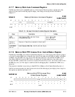
21.7.5 Memory Stick Parallel Port Control/Data Register
The Memory Stick Parallel Port Control/Data Register is a 16-bit register. The bit position assignments for
this register are shown in the following register display. The settings for this register are described in
Table 21-12.
This register is initialized on power up or when RST bit of Memory Stick Control/Status Register is 1.
Parallel input MS_PIN [1:0] is configured using two flip-flops each running at 1/16 clock.
•
The parallel input pin MS_PI [1:0] is pulled up internally.
•
The XPIN [1:0] bit is 1
when the MS_PI [1:0] pin is Low level, and 0 when High level.
It takes 30 HCLK cycles for a value from the parallel input pin PI [1:0] to be reflected on bits XPIN
[1:0].This detection is available in following conditions:
•
MC9328MX1 is in Normal operation mode or Doze mode and the MSHC module must be enabled
(MSCEN bit is set).
•
Under the above condition, MSHC module is in Normal operation mode (PWS bit = 0) or Power
Save Mode (PWS bit = 1).
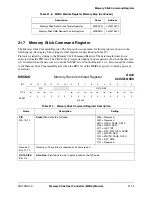
TOE
Bit 0
Time-Out Error
—Indicates that a BSY time-out error occurred. Cleared
when data is written to the Memory Stick Command Register. Exceeding
the number of clocks set using BSYCNT of the Control register is taken
as a card malfunction and an RDY time-out error (TOE) is sent out. Also,
RDY becomes 1 and an interrupt signal is output.
An internal interrupt request (MSIRQ) for this bit is negated by reading
the MSICS register (when INTEN = 1).
0 = No BSY time-out error
1 = BSY time-out error
MSPPCD
Memory Stick Parallel Port Control/Data
Register
Addr
0x0021A008
BIT
15
14
13
12
11
10
9
8
7
6
5
4
3
2
1
0
PIEN1
PIEN0
XPIN1
XPIN0
TYPE
r
r
rw
rw
r
r
r
r
r
r
r
r
r
r
r
r
RESET
0
0
0
0
0
0
0
0
0
0
0
0
0
0
0
0
0x0000
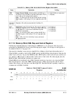
Table 21-12. Memory Stick Parallel Port Control/Data Register Description
Name
Description
Setting
Reserved
Bits 15–14
Reserved—These bits are reserved and should read 0.
PIEN1
Bit 13
PIEN1
—Enables/Disables parallel port data input on
MS_PI1.
0 = Parallel input port disabled
1 = Parallel input port enabled
PIEN0
Bit 12
PIEN0
—Enables/Disables parallel port data input on
MS_PI0.
0 = Parallel input port disabled
1 = Parallel input port enabled
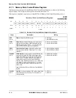
Table 21-11. Memory Stick Interrupt Control/Status Register Description (Continued)
Name
Description
Setting
Summary of Contents for DragonBall MC9328MX1
Page 68: ...1 12 MC9328MX1 Reference Manual MOTOROLA Introduction ...
Page 86: ...2 18 MC9328MX1 Reference Manual MOTOROLA Signal Descriptions and Pin Assignments ...
Page 116: ...3 30 MC9328MX1 Reference Manual MOTOROLA Memory Map ...
Page 126: ...4 10 MC9328MX1 Reference Manual MOTOROLA ARM920T Processor ...
Page 160: ...8 8 MC9328MX1 Reference Manual MOTOROLA System Control ...
Page 272: ...13 32 MC9328MX1 Reference Manual MOTOROLA DMA Controller ...
Page 281: ...Programming Model MOTOROLA Watchdog Timer Module 14 9 ...
Page 282: ...14 10 MC9328MX1 Reference Manual MOTOROLA Watchdog Timer Module ...
Page 300: ...15 18 MC9328MX1 Reference Manual MOTOROLA Analog Signal Processor ASP ...
Page 438: ...18 16 MC9328MX1 Reference Manual MOTOROLA Serial Peripheral Interface Modules SPI 1 and SPI 2 ...
Page 478: ...19 40 MC9328MX1 Reference Manual MOTOROLA LCD Controller ...
Page 574: ...21 32 MC9328MX1 Reference Manual MOTOROLA Memory Stick Host Controller MSHC Module ...
Page 598: ...23 16 MC9328MX1 Reference Manual MOTOROLA Real Time Clock RTC ...
Page 670: ...24 72 MC9328MX1 Reference Manual MOTOROLA SDRAM Memory Controller ...
Page 726: ...25 56 MC9328MX1 Reference Manual MOTOROLA SmartCard Interface Module SIM ...
Page 736: ...26 10 MC9328MX1 Reference Manual MOTOROLA General Purpose Timers ...
Page 854: ...29 18 MC9328MX1 Reference Manual MOTOROLA I2C Module ...
Page 900: ...30 46 MC9328MX1 Reference Manual MOTOROLA Synchronous Serial Interface SSI ...
Page 942: ...32 26 MC9328MX1 Reference Manual MOTOROLA GPIO Module and I O Multiplexer IOMUX ...

