24-26
MC9328MX1 Reference Manual
MOTOROLA
SDRAM Memory Controller
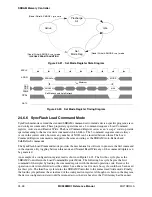
Figure 24-21. Set Mode Register State Diagram
Figure 24-22. Set Mode Register Timing Diagram
24.6.6 SyncFlash Load Command Mode
SyncFlash memories extend the standard SDRAM command set to include device-specific program, erase,
and configure commands. These proprietary operations use a 3 command sequence: Load Command
register, Activate, and Read or Write. The Load Command Register serves as an “escape” code to provide
special meaning to the read or write commands which follow. The 3 command sequences must always
occur in the correct order, however any number of NOPs can be inserted between them. The Load
Command Register command is mapped to the same encoding as the SDRAM Auto-Refresh and
Self-Refresh commands.
The SyncFlash Load Command mode provides the mechanism for software to generate the first command
in the sequence. By toggling between this mode and Normal Read/Write any of the command triplets can
be generated.
An example of a configuration register read is shown in Figure 24-23. The first bus cycle places the
SDRAM Controller in the Load Command Register Mode. The following bus cycle begins the first
command of the triplet by loading the command register with the desired operation code. Because the
operation code is transferred across the address bus, either a read or write bus cycle could have been used
for this cycle. The third bus cycle returns the SDRAM Controller to the normal read/write mode. Finally,
the fourth cycle performs the actual read of the configuration register. Although not shown in the diagram,
the device configuration data would be returned across the data bus after the CAS latency had been met.
Precharge
All
Set
Mode Reg
Active
Idle
(Read | Write) & SMODE = pre_cmd
(Read | Write) & SMODE = set_mode
(Read | Write) & SMODE = set_mode
ILLEGAL SDRAM TRANSITION
SDRAMx
SDCLK
RAS,
CAS,
SDWE
CSDx
DATA
ADDR
t
RC
Minimum
MODE
REFRESH
MRS
Self-Refresh and Auto-Refresh
Summary of Contents for DragonBall MC9328MX1
Page 68: ...1 12 MC9328MX1 Reference Manual MOTOROLA Introduction ...
Page 86: ...2 18 MC9328MX1 Reference Manual MOTOROLA Signal Descriptions and Pin Assignments ...
Page 116: ...3 30 MC9328MX1 Reference Manual MOTOROLA Memory Map ...
Page 126: ...4 10 MC9328MX1 Reference Manual MOTOROLA ARM920T Processor ...
Page 160: ...8 8 MC9328MX1 Reference Manual MOTOROLA System Control ...
Page 272: ...13 32 MC9328MX1 Reference Manual MOTOROLA DMA Controller ...
Page 281: ...Programming Model MOTOROLA Watchdog Timer Module 14 9 ...
Page 282: ...14 10 MC9328MX1 Reference Manual MOTOROLA Watchdog Timer Module ...
Page 300: ...15 18 MC9328MX1 Reference Manual MOTOROLA Analog Signal Processor ASP ...
Page 438: ...18 16 MC9328MX1 Reference Manual MOTOROLA Serial Peripheral Interface Modules SPI 1 and SPI 2 ...
Page 478: ...19 40 MC9328MX1 Reference Manual MOTOROLA LCD Controller ...
Page 574: ...21 32 MC9328MX1 Reference Manual MOTOROLA Memory Stick Host Controller MSHC Module ...
Page 598: ...23 16 MC9328MX1 Reference Manual MOTOROLA Real Time Clock RTC ...
Page 670: ...24 72 MC9328MX1 Reference Manual MOTOROLA SDRAM Memory Controller ...
Page 726: ...25 56 MC9328MX1 Reference Manual MOTOROLA SmartCard Interface Module SIM ...
Page 736: ...26 10 MC9328MX1 Reference Manual MOTOROLA General Purpose Timers ...
Page 854: ...29 18 MC9328MX1 Reference Manual MOTOROLA I2C Module ...
Page 900: ...30 46 MC9328MX1 Reference Manual MOTOROLA Synchronous Serial Interface SSI ...
Page 942: ...32 26 MC9328MX1 Reference Manual MOTOROLA GPIO Module and I O Multiplexer IOMUX ...


