24-28
MC9328MX1 Reference Manual
MOTOROLA
SDRAM Memory Controller
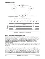
A write to an address within the memory region initiates the program sequence. The first command issued
to the SyncFlash is Load Command register. A [7:0] determines which operation the command performs.
For this write setup operation, an address of 0x40 is hardware generated. The bank and other address lines
are driven with the address to be programmed. The second command, Active, registers the row address and
confirms the bank address. The third command supplies the column address, re-confirms the bank address,
and supplies the data to be written. SyncFlash does not support burst writes, therefore a Burst Terminate
command is not required.
A read to the memory region initiates the status read sequence. The first command issued to the SyncFlash
is the Load Command Register with A [7:0] set to 0x70 which corresponds to the Read Status Register
operation. The bank and other address lines are driven to the selected address. The second command,
Active, sets up the status register read. The bank and row addresses are driven during this command. The
third command of the triplet is Read. Bank and column addresses are driven on the address bus during this
command. Data is returned from memory on the low-order 8 data bits following the CAS latency.
Figure 24-25. SyncFlash Program Timing Diagram
Figure 24-26. SyncFlash Read Status Register Timing Diagram
24.7 General Operation
The general operation of the SDRAM controller is discussed in this section and includes address
multiplexing, refresh and self-refresh modes. The SDRAM Controller is designed to support a broad range
of JEDEC standard SDRAM configurations including devices of 64-, 128-, and 256-Mbit densities. Given
SDCLK
RAS, CAS, SDWE
CSDx
DATA
ADDR
LCR
ACT
WRIT
BANK
A
, CMD BANK/ROW
A
COLUMN
A
DATA
A
SDCLK
RAS,
CAS,
SDWE
CSDx
DATA
ADDR
DATA
A
BANK
A
, CMD BANK/ROW
A
COLUMN
A
LCR
ACT
READ
t
CL
= 2
Summary of Contents for DragonBall MC9328MX1
Page 68: ...1 12 MC9328MX1 Reference Manual MOTOROLA Introduction ...
Page 86: ...2 18 MC9328MX1 Reference Manual MOTOROLA Signal Descriptions and Pin Assignments ...
Page 116: ...3 30 MC9328MX1 Reference Manual MOTOROLA Memory Map ...
Page 126: ...4 10 MC9328MX1 Reference Manual MOTOROLA ARM920T Processor ...
Page 160: ...8 8 MC9328MX1 Reference Manual MOTOROLA System Control ...
Page 272: ...13 32 MC9328MX1 Reference Manual MOTOROLA DMA Controller ...
Page 281: ...Programming Model MOTOROLA Watchdog Timer Module 14 9 ...
Page 282: ...14 10 MC9328MX1 Reference Manual MOTOROLA Watchdog Timer Module ...
Page 300: ...15 18 MC9328MX1 Reference Manual MOTOROLA Analog Signal Processor ASP ...
Page 438: ...18 16 MC9328MX1 Reference Manual MOTOROLA Serial Peripheral Interface Modules SPI 1 and SPI 2 ...
Page 478: ...19 40 MC9328MX1 Reference Manual MOTOROLA LCD Controller ...
Page 574: ...21 32 MC9328MX1 Reference Manual MOTOROLA Memory Stick Host Controller MSHC Module ...
Page 598: ...23 16 MC9328MX1 Reference Manual MOTOROLA Real Time Clock RTC ...
Page 670: ...24 72 MC9328MX1 Reference Manual MOTOROLA SDRAM Memory Controller ...
Page 726: ...25 56 MC9328MX1 Reference Manual MOTOROLA SmartCard Interface Module SIM ...
Page 736: ...26 10 MC9328MX1 Reference Manual MOTOROLA General Purpose Timers ...
Page 854: ...29 18 MC9328MX1 Reference Manual MOTOROLA I2C Module ...
Page 900: ...30 46 MC9328MX1 Reference Manual MOTOROLA Synchronous Serial Interface SSI ...
Page 942: ...32 26 MC9328MX1 Reference Manual MOTOROLA GPIO Module and I O Multiplexer IOMUX ...


