24-32
MC9328MX1 Reference Manual
MOTOROLA
SDRAM Memory Controller
24.7.1.3 Bank Addresses
Which bank addresses of the SDRAM controller are multiplexed with which MC9328MX1 address pins,
depends on whether or not the memory system is in interleaved mode. For non-interleaved mode, the
SDRAM controller bank addresses SDBA[4:0] are multiplexed with the address pins A[15:11]. For
interleaved mode, the SDRAM controller “interleaved” bank addresses SDIBA[3:0] are multiplexed with
the MC9328MX1 address pins A[19:16]. Instead of detailing the complexity of how these bank addresses
are multiplexed with the corresponding MC9328MX1 address pins with different memory configurations,
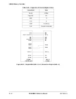
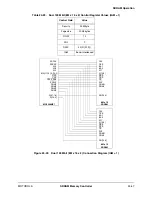
the user is directed to Table 24-14. This table explicitly shows which SDRAM memory bank address pin
must be connected to which corresponding MC9328MX1 address pins given different the JEDEC standard
memory configurations. Also, if the user wants to derive how the density of the memory is calculated or
how to derive the page size, they use the following equations:
Page Size (Bytes) = 2
#Column Address Bits
× (Memory Width in Bits / 8)
Eqn. 24-1
Density (Bytes) = 2
(# Column Address Bits + # Row Address Bits)
× (Memory Width in Bits / 2)
Eqn. 24-2
24.7.2 Refresh
SDRAM Controller hardware satisfies all SDRAM refresh requirements after an initial configuration by
the user software. 0, 1, 2, or 4 refresh cycles are scheduled at 31.25
µ
S (nominal 32 kHz clock) intervals,
providing 0, 2048, 4096, or 8192 refresh cycles every 64 ms. The refresh rate is programmed through the
SREFR field in the SDCTLx registers. Each array can have a different rate, allowing a mix of different
density SDRAMs. Refresh is disabled by hardware reset.
A refresh request is made pending at each rising edge on the 32 kHz clock. In response to this request, the
hardware gains control of the SDRAM as soon as any in-process bus cycle completes. Once it has gained
control of the memory, commands are issued to precharge all banks. Following a row precharge delay
(t
RP
), an auto-refresh command is issued. At t
RC
intervals, additional auto-refresh cycles are issued until
the specified number of cycles have been run. Figure 24-27 illustrates a 2 refresh sequence.
Burst transfers in progress when the refresh request arrives are allowed to complete prior to the refresh
operation. SDRAM bus accesses queued after the refresh request are held off until the refresh completes.
In Figure 24-28, an access is queued just as the refresh begins. This cycle is delayed until the precharge
and single refresh (SREFR = 01) cycles are run. Bus cycles targeted to other memory or peripheral devices
are allowed to progress normally while the refresh is in progress. None of the pins shared between the
SDRAM and other devices are required for the refresh operation.
Figure 24-27. Hardware Refresh Timing Diagram
SDCLK
ADDR
RAS,
CAS,
SDWE
CSDx
DATA
DATA
A
A10 = 1
PRE-ALL
REF A
REF A
>= t
RP
>= t
RC
32KHz
Summary of Contents for DragonBall MC9328MX1
Page 68: ...1 12 MC9328MX1 Reference Manual MOTOROLA Introduction ...
Page 86: ...2 18 MC9328MX1 Reference Manual MOTOROLA Signal Descriptions and Pin Assignments ...
Page 116: ...3 30 MC9328MX1 Reference Manual MOTOROLA Memory Map ...
Page 126: ...4 10 MC9328MX1 Reference Manual MOTOROLA ARM920T Processor ...
Page 160: ...8 8 MC9328MX1 Reference Manual MOTOROLA System Control ...
Page 272: ...13 32 MC9328MX1 Reference Manual MOTOROLA DMA Controller ...
Page 281: ...Programming Model MOTOROLA Watchdog Timer Module 14 9 ...
Page 282: ...14 10 MC9328MX1 Reference Manual MOTOROLA Watchdog Timer Module ...
Page 300: ...15 18 MC9328MX1 Reference Manual MOTOROLA Analog Signal Processor ASP ...
Page 438: ...18 16 MC9328MX1 Reference Manual MOTOROLA Serial Peripheral Interface Modules SPI 1 and SPI 2 ...
Page 478: ...19 40 MC9328MX1 Reference Manual MOTOROLA LCD Controller ...
Page 574: ...21 32 MC9328MX1 Reference Manual MOTOROLA Memory Stick Host Controller MSHC Module ...
Page 598: ...23 16 MC9328MX1 Reference Manual MOTOROLA Real Time Clock RTC ...
Page 670: ...24 72 MC9328MX1 Reference Manual MOTOROLA SDRAM Memory Controller ...
Page 726: ...25 56 MC9328MX1 Reference Manual MOTOROLA SmartCard Interface Module SIM ...
Page 736: ...26 10 MC9328MX1 Reference Manual MOTOROLA General Purpose Timers ...
Page 854: ...29 18 MC9328MX1 Reference Manual MOTOROLA I2C Module ...
Page 900: ...30 46 MC9328MX1 Reference Manual MOTOROLA Synchronous Serial Interface SSI ...
Page 942: ...32 26 MC9328MX1 Reference Manual MOTOROLA GPIO Module and I O Multiplexer IOMUX ...


