SDRAM Operation
MOTOROLA
SDRAM Memory Controller
24-57
6. SDRAM is now ready for normal operation.
The SDRAM Controller accomplishes steps 1 and 2 in hardware, however it relies on software assistance
to complete the remaining actions. The 200
µ
s stabilization period is guaranteed by the use of 2 reset
signals whose negations are separated by this amount. An SDRAM reset signal (SD_RST) is asserted to
coincide with the system reset used by the rest of the chip, however it negates 200 ms prior to the negation
of system reset. The SDRAM Controller leaves the SDRAM arrays in a NOP condition following the
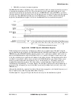
negation of the DRAM reset. Figure 24-53 shows the SDRAM Power-on initialization sequence.
Figure 24-53. SDRAM Power-On Initialization Sequence
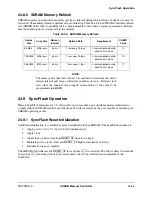
Following negation of system reset, initialization software must complete steps 3 through 5 using the
special operating modes enabled by the SMODE field in the SDRAM Control Register. To precharge the
SDRAM array, the SDRAM Controller operating mode is set to “precharge command” and an access is
made to the SDRAM address range with address bit A10 = 1. Instead of running a normal read or write
cycle, the controller issues a precharge all command to the addressed array. The operating mode is then
switched to “auto-refresh” and 8 accesses are made to the SDRAM address space. Each of the accesses
results in a refresh command to the addressed array. A “mode register set” command is required to
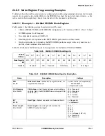
complete the initialization sequence. The value written is system dependent. Consult Section 24.8.4,
“Mode Register Programming,” for details. Finally, the controller is placed back in the normal mode of
operation so that subsequent accesses to the address space result in normal read and write cycles to the
SDRAM array.
Although the initialization sequence described in the previous paragraphs is only required at power-on, it
may be repeated at any time the programmer deems necessary.
Code Example 24-2 on page 24-58 provides the code necessary for the initialization sequence.
NOP
PRE
ALL
AUTO
REF
NORMAL
AUTO
REF
AUTO
REF
AUTO
REF
AUTO
REF
AUTO
REF
AUTO
REF
AUTO
REF
MODE
SET
200
µ
s Minimum
SDRAM Software Initialization Sequence
VCC
SYSTEM
CLOCK
DRAM
RESET
HARD_ASYN_
RESET
SDCLK
SDRAM
COMMAND
Summary of Contents for DragonBall MC9328MX1
Page 68: ...1 12 MC9328MX1 Reference Manual MOTOROLA Introduction ...
Page 86: ...2 18 MC9328MX1 Reference Manual MOTOROLA Signal Descriptions and Pin Assignments ...
Page 116: ...3 30 MC9328MX1 Reference Manual MOTOROLA Memory Map ...
Page 126: ...4 10 MC9328MX1 Reference Manual MOTOROLA ARM920T Processor ...
Page 160: ...8 8 MC9328MX1 Reference Manual MOTOROLA System Control ...
Page 272: ...13 32 MC9328MX1 Reference Manual MOTOROLA DMA Controller ...
Page 281: ...Programming Model MOTOROLA Watchdog Timer Module 14 9 ...
Page 282: ...14 10 MC9328MX1 Reference Manual MOTOROLA Watchdog Timer Module ...
Page 300: ...15 18 MC9328MX1 Reference Manual MOTOROLA Analog Signal Processor ASP ...
Page 438: ...18 16 MC9328MX1 Reference Manual MOTOROLA Serial Peripheral Interface Modules SPI 1 and SPI 2 ...
Page 478: ...19 40 MC9328MX1 Reference Manual MOTOROLA LCD Controller ...
Page 574: ...21 32 MC9328MX1 Reference Manual MOTOROLA Memory Stick Host Controller MSHC Module ...
Page 598: ...23 16 MC9328MX1 Reference Manual MOTOROLA Real Time Clock RTC ...
Page 670: ...24 72 MC9328MX1 Reference Manual MOTOROLA SDRAM Memory Controller ...
Page 726: ...25 56 MC9328MX1 Reference Manual MOTOROLA SmartCard Interface Module SIM ...
Page 736: ...26 10 MC9328MX1 Reference Manual MOTOROLA General Purpose Timers ...
Page 854: ...29 18 MC9328MX1 Reference Manual MOTOROLA I2C Module ...
Page 900: ...30 46 MC9328MX1 Reference Manual MOTOROLA Synchronous Serial Interface SSI ...
Page 942: ...32 26 MC9328MX1 Reference Manual MOTOROLA GPIO Module and I O Multiplexer IOMUX ...


