24-66
MC9328MX1 Reference Manual
MOTOROLA
SDRAM Memory Controller
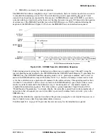
Figure 24-54. Sync Flash Reset Timing
24.9.2 SyncFlash Mode Register Programming
The mode register can be programmed following the initialization sequence, although it is generally not
required. A non-volatile mode register is initially programmed at the same time as the rest of the array.
This non-volatile register is copied into the mode register automatically during device initialization, and
does not require reloading prior to the first operational command. Software may overwrite the default
value at any time the memory is idle using the same sequence as an SDRAM mode register. Consult
Section 24.8.4, “Mode Register Programming,” for details.
Programming the SyncFlash non-volatile mode register requires a specialized sequence of load command
register triplets with VccP applied. Consult the SyncFlash data sheet for details.
24.9.3 Booting From SyncFlash
The SDRAM Controller is designed to permit booting from the SyncFlash device immediately out of reset.
Default values in the configuration register allow booting at frequencies up to 100 MHz. Complete
initialization of the controller is still required, however, and must be completed as quickly as possible.
24.9.4 SyncFlash Configuration
Hardware connections are similar to those for SDRAM of like density. One difference is that a SyncFlash
boot device is limited to using CSD1. SyncFlash can be connected to CSD0, however, it cannot be the boot
device. The second difference is the added connection to the reset/powerdown pin (RESET_SF). An
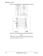
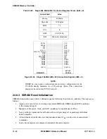
example of a 32-bit configuration is provided in Figure 24-56.
The only significant difference in the software configuration is that refresh
must
be disabled. SyncFlash
maps the control register access commands to the same basic commands as SDRAM refresh. Enabling
hardware refresh would most likely result in unexpected behavior.
NOP
100
µ
S Minimum
VCC
SYSTEM
CLOCK
DRAM
RESET
SYSTEM
RESET
SDCLK
SYNCFLASH
COMMAND
RESET_SF
Vector Fetch
Instruction Fetches
ACT
READ READ
Summary of Contents for DragonBall MC9328MX1
Page 68: ...1 12 MC9328MX1 Reference Manual MOTOROLA Introduction ...
Page 86: ...2 18 MC9328MX1 Reference Manual MOTOROLA Signal Descriptions and Pin Assignments ...
Page 116: ...3 30 MC9328MX1 Reference Manual MOTOROLA Memory Map ...
Page 126: ...4 10 MC9328MX1 Reference Manual MOTOROLA ARM920T Processor ...
Page 160: ...8 8 MC9328MX1 Reference Manual MOTOROLA System Control ...
Page 272: ...13 32 MC9328MX1 Reference Manual MOTOROLA DMA Controller ...
Page 281: ...Programming Model MOTOROLA Watchdog Timer Module 14 9 ...
Page 282: ...14 10 MC9328MX1 Reference Manual MOTOROLA Watchdog Timer Module ...
Page 300: ...15 18 MC9328MX1 Reference Manual MOTOROLA Analog Signal Processor ASP ...
Page 438: ...18 16 MC9328MX1 Reference Manual MOTOROLA Serial Peripheral Interface Modules SPI 1 and SPI 2 ...
Page 478: ...19 40 MC9328MX1 Reference Manual MOTOROLA LCD Controller ...
Page 574: ...21 32 MC9328MX1 Reference Manual MOTOROLA Memory Stick Host Controller MSHC Module ...
Page 598: ...23 16 MC9328MX1 Reference Manual MOTOROLA Real Time Clock RTC ...
Page 670: ...24 72 MC9328MX1 Reference Manual MOTOROLA SDRAM Memory Controller ...
Page 726: ...25 56 MC9328MX1 Reference Manual MOTOROLA SmartCard Interface Module SIM ...
Page 736: ...26 10 MC9328MX1 Reference Manual MOTOROLA General Purpose Timers ...
Page 854: ...29 18 MC9328MX1 Reference Manual MOTOROLA I2C Module ...
Page 900: ...30 46 MC9328MX1 Reference Manual MOTOROLA Synchronous Serial Interface SSI ...
Page 942: ...32 26 MC9328MX1 Reference Manual MOTOROLA GPIO Module and I O Multiplexer IOMUX ...


