Programming Model
MOTOROLA
Universal Asynchronous Receiver/Transmitters (UART) Modules
27-33
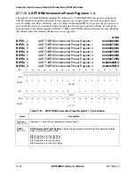
27.7.5.2 UART2 Control Register 3
UCR3_2
UART2 Control Register 3
Addr
0x00207088
BIT
31
30
29
28
27
26
25
24
23
22
21
20
19
18
17
16
TYPE
r
r
r
r
r
r
r
r
r
r
r
r
r
r
r
r
RESET
0
0
0
0
0
0
0
0
0
0
0
0
0
0
0
0
0x0000
BIT
15
14
13
12
11
10
9
8
7
6
5
4
3
2
1
0
DPEC
DTR
EN
PARERR
EN
FRAERR
EN
DSR DCD RI
RXDS
EN
AIR
INT
EN
AWAK
EN
REF25 REF30 INVT BPEN
TYPE
rw
rw
rw
rw
rw
rw
rw
rw
r
rw
rw
rw
rw
rw
rw
rw
RESET
0
0
0
0
0
0
0
0
0
0
0
0
0
0
0
0
0x0000
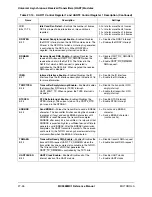
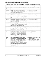
Table 27-17. UART1 Control Register 3 and UART2 Control Register 3 Description
Name
Description
Settings
Reserved
Bits 31–16
Reserved—These bits are reserved and should read 0.
DPEC
Bits 15–14
DTR Interrupt Edge Control
—Controls the edge
that generates an interrupt. An interrupt is generated
only if the DTREN bit is set.
00 = Interrupt generated on rising edge
01 = Interrupt generated on falling edge
1X = Interrupt generated on either edge
DTREN
Bit 13
Data Terminal Ready Interrupt Enable
—Controls
the DTR edge sensitive interrupt. When DTREN is
asserted and the programmed edge is detected on
the UART2_DTR pin, the DTRF bit is asserted (see
Table 27-4).
0 = Disable the data terminal ready
interrupt
1 = Enable the data terminal ready interrupt
PARERREN
Bit 12
Parity Error Interrupt Enable
—Enables/Disables
the interrupt. When asserted, PARERREN causes
the PARITYERR bit to generate an interrupt
(UART_MINT_PFERR
=
0)
0 = Disable the parity error interrupt
1 = Enable the parity error interrupt
FRAERREN
Bit 11
Frame Error Interrupt Enable
—Enables/Disables
the interrupt. When asserted, FRAERREN causes
the FRAMERR bit to generate an interrupt
(UART_MINT_PFERR
=
0)
0 = Disable the frame error interrupt
1 = Enable the frame error interrupt
DSR
Bit 10
Data Set Ready
—Selects the logic level for the
UART_DSR pin for the modem interface.
0 = The UART_DSR pin is logic 0
1 = The UART_DSR pin is logic 1
DCD
Bit 9
Data Carrier Detect
—Selects the logic level for the
UART_DCD pin for the modem interface.
0 = The UART_DCD pin is logic 0
1 = The UART_DCD pin is logic 1
RI
Bit 8
Ring Indicator
—Selects the logic level for the
UART_RI pin for the modem interface.
0 = The UART_RI pin is logic 0
1 = The UART_RI pin is logic 1
Summary of Contents for DragonBall MC9328MX1
Page 68: ...1 12 MC9328MX1 Reference Manual MOTOROLA Introduction ...
Page 86: ...2 18 MC9328MX1 Reference Manual MOTOROLA Signal Descriptions and Pin Assignments ...
Page 116: ...3 30 MC9328MX1 Reference Manual MOTOROLA Memory Map ...
Page 126: ...4 10 MC9328MX1 Reference Manual MOTOROLA ARM920T Processor ...
Page 160: ...8 8 MC9328MX1 Reference Manual MOTOROLA System Control ...
Page 272: ...13 32 MC9328MX1 Reference Manual MOTOROLA DMA Controller ...
Page 281: ...Programming Model MOTOROLA Watchdog Timer Module 14 9 ...
Page 282: ...14 10 MC9328MX1 Reference Manual MOTOROLA Watchdog Timer Module ...
Page 300: ...15 18 MC9328MX1 Reference Manual MOTOROLA Analog Signal Processor ASP ...
Page 438: ...18 16 MC9328MX1 Reference Manual MOTOROLA Serial Peripheral Interface Modules SPI 1 and SPI 2 ...
Page 478: ...19 40 MC9328MX1 Reference Manual MOTOROLA LCD Controller ...
Page 574: ...21 32 MC9328MX1 Reference Manual MOTOROLA Memory Stick Host Controller MSHC Module ...
Page 598: ...23 16 MC9328MX1 Reference Manual MOTOROLA Real Time Clock RTC ...
Page 670: ...24 72 MC9328MX1 Reference Manual MOTOROLA SDRAM Memory Controller ...
Page 726: ...25 56 MC9328MX1 Reference Manual MOTOROLA SmartCard Interface Module SIM ...
Page 736: ...26 10 MC9328MX1 Reference Manual MOTOROLA General Purpose Timers ...
Page 854: ...29 18 MC9328MX1 Reference Manual MOTOROLA I2C Module ...
Page 900: ...30 46 MC9328MX1 Reference Manual MOTOROLA Synchronous Serial Interface SSI ...
Page 942: ...32 26 MC9328MX1 Reference Manual MOTOROLA GPIO Module and I O Multiplexer IOMUX ...


