DSP Core Programming Model
Host Interface (HI08)
6
-15
6.6.2
Host Status Register (HSR)
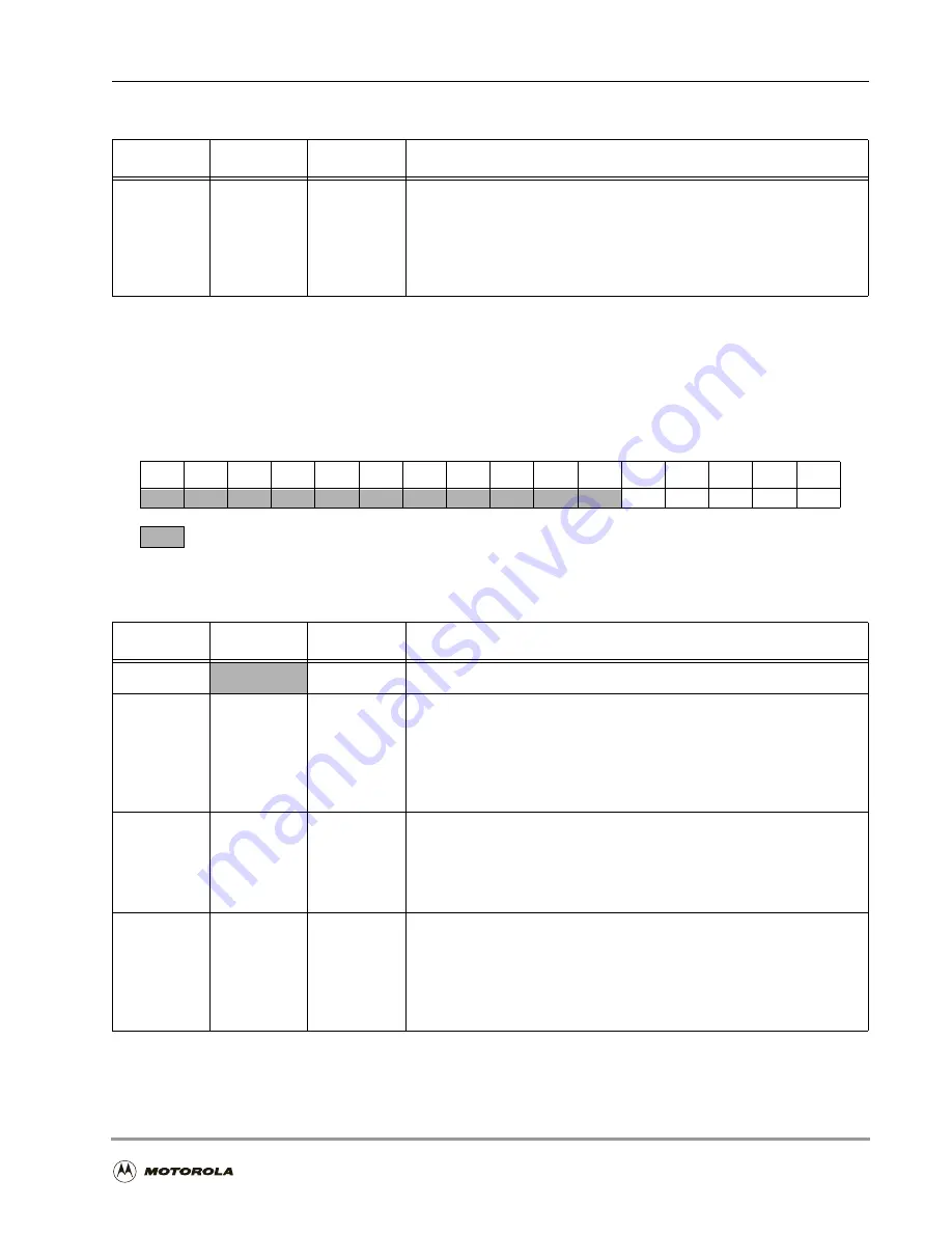
The HSR is a 16-bit read-only status register by which the DSP reads the HI08 status and
flags. The host processor cannot access it directly. The initialization values for the HSR bits
are discussed in Section 6.6.9, DSP-Side Registers After Reset, on page 6-22.
0
HRIE
0
Host Receive Interrupt Enable
Generates a host receive data interrupt request if the host receive data full
(HRDF) bit in the host status register (HSR, Bit 0) is set. The HRDF bit is
set when data is transferred to the HRX from the TXH, TXM, or TXL
registers. If HRIE is cleared, HRDF interrupts are disabled. The bit value is
indeterminate after an individual reset.
15
14
13
12
11
10
9
8
7
6
5
4
3
2
1
0
HF1
HF0
HCP HTDE HRDF
—Reserved bit; read as 0; write to 0 for future compatibility.
Figure 6-7. Host Status Register (HSR) (X:$FFFFC3)
Table 6-9. Host Status Register (HSR) Bit Definitions
Bit Number
Bit Name
Reset Value
Description
15–5
0
Reserved. Write to 0 for future compatibility.
4–3
HF[1–0]
0
Host Flags 0, 1
General-purpose flags for host-to-DSP communication. These bits reflect
the status of host flags HF[1–0] in the ICR on the host side. These two
general-purpose flags can be used individually or as encoded pairs in a
simple host-to-DSP communication protocol, implemented in both the
DSP and the host processor software.
2
HCP
0
Host Command Pending
Reflects the status of the CVR[HC] bit. When set, it indicates that a host
command interrupt is pending. HI08 hardware clears HC and HCP when
the DSP core services the interrupt request. If the host clears HC, HCP is
also cleared.
1
HTDE
0
Host Transmit Data Empty
Indicates that the host transmit data register (HTX) is empty and can be
written by the DSP core. HTDE is set when the HTX register is transferred
to the RXH:RXM:RXL registers. The host processor can also set HTDE
using the initialize function. HTDE is cleared when the DSP core writes to
HTX.
Table 6-8. Host Control Register (HCR) Bit Definitions
Bit Number
Bit Name
Reset Value
Description
Summary of Contents for DSP56303
Page 1: ...DSP56303 User s Manual 24 Bit Digital Signal Processor DSP56303UM AD Revision 1 January 2001 ...
Page 52: ...JTAG OnCE Interface 2 22 DSP56303 User s Manual ...
Page 114: ...General Purpose Input Output GPIO 5 10 DSP56303 User s Manual ...
Page 212: ...GPIO Signals and Registers 8 26 DSP56303 User s Manual ...
Page 268: ...Interrupt Equates A 22 DSP56303 User s Manual ...
Page 306: ...Programming Sheets B 38 DSP56303 User s Manual ...
Page 320: ...Index 14 DSP56303 User s Manual ...


