ESSI Programming Model
Enhanced Synchronous Serial Interface (ESSI)
7
-35
7.5.10
Receive Slot Mask Registers (RSMA, RSMB)
Both receive slot mask registers are read/write registers. In Network mode, the receiver(s) use
these registers to determine which action to take in the current time slot. Depending on the
setting of the bits, the receiver(s) either tri-state the receiver(s) data signal(s) or receive a data
word and generate a receiver full condition.
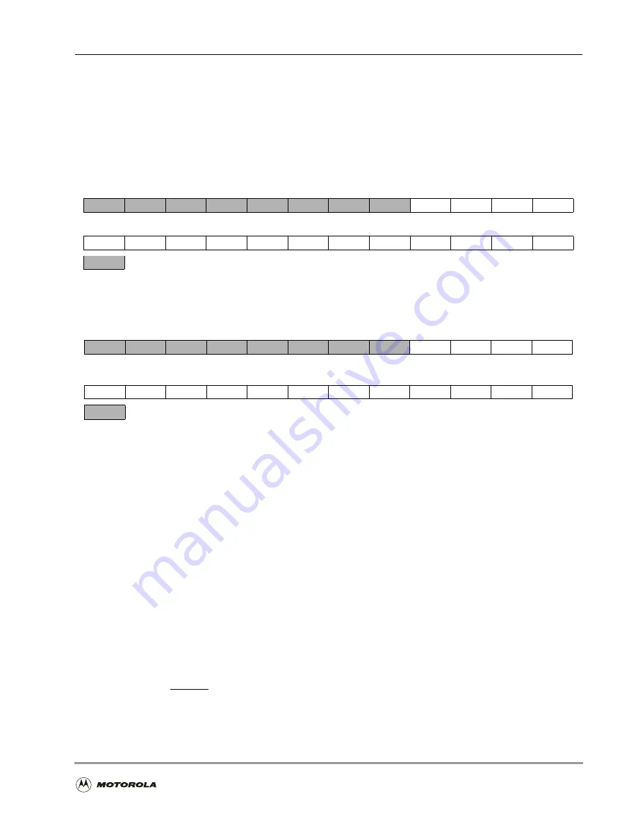
RSMA and RSMB (as in Figure 7-12 and Figure 7-13) can be seen as one 32-bit register,
RSM. Bit n in RSM (RSn) is an enable/disable control bit for time slot number N. When RSn
is cleared, all the data signals of the enabled receivers are tri-stated during time slot number
N. Data transfers from the receive data register(s) to the receive shift register(s), but the RDF
and ROE flags are not set. Consequently, during a disabled slot, no receiver full interrupt is
generated. The DSP is interrupted only for enabled slots. When RSn is set, the receive
sequence proceeds normally. Data is received during slot number N, and the RDF flag is set.
When the bits in the RSM are set, their setting affects the next frame transmission. The frame
being transmitted is not affected by the new RSM setting. If the RSM is read, it shows the
current setting.
When RSMA or RSMB is read by the internal data bus, the register contents occupy the two
low-order bytes of the data bus, and the high-order byte is filled by 0.
After a hardware
RESET
signal or a software RESET instruction, the RSM register is reset to
$FFFFFFFF, enabling all 32 time slots for data transmission.
23
22
21
20
19
18
17
16
15
14
13
12
RS15
RS14
RS13
RS12
11
10
9
8
7
6
5
4
3
2
1
0
RS11
RS10
RS9
RS8
RS7
RS6
RS5
RS4
RS3
RS2
RS1
RS0
—Reserved bit; read as 0; write to 0 0 for future compatibility.
(ESSI0 X:$FFFFB2, ESSI1 X:$FFFFA2)
Figure 7-16. ESSI Receive Slot Mask Register A (RSMA)
23
22
21
20
19
18
17
16
15
14
13
12
RS31
RS30
RS29
RS28
11
10
9
8
7
6
5
4
3
2
1
0
RS27
RS26
RS25
RS24
RS23
RS22
RS21
RS20
RS19
RS18
RS17
RS16
–Reserved. Read as zero. Write with zero for future compatibility.
(ESSI0 X:$FFFFB1, ESSI1 X:$FFFFA1)
Figure 7-17. ESSI Receive Slot Mask Register B (RSMB)
Summary of Contents for DSP56303
Page 1: ...DSP56303 User s Manual 24 Bit Digital Signal Processor DSP56303UM AD Revision 1 January 2001 ...
Page 52: ...JTAG OnCE Interface 2 22 DSP56303 User s Manual ...
Page 114: ...General Purpose Input Output GPIO 5 10 DSP56303 User s Manual ...
Page 212: ...GPIO Signals and Registers 8 26 DSP56303 User s Manual ...
Page 268: ...Interrupt Equates A 22 DSP56303 User s Manual ...
Page 306: ...Programming Sheets B 38 DSP56303 User s Manual ...
Page 320: ...Index 14 DSP56303 User s Manual ...