SCI Programming Model
Serial Communication Interface (SCI)
8
-19
8.6.3
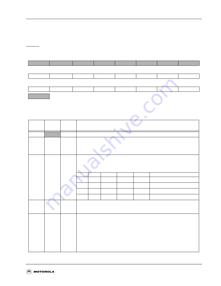
SCI Clock Control Register (SCCR)
The SCCR is a read/write register that controls the selection of clock modes and baud rates for
the transmit and receive sections of the SCI interface. The SCCR is cleared by a hardware
RESET
signal.
23
22
21
20
19
18
17
16
15
14
13
12
11
10
9
8
TCM
RCM
SCP
COD
CD11
CD10
CD9
CD8
7
6
5
4
3
2
1
0
CD7
CD6
CD5
CD4
CD3
CD2
CD1
CD0
Reserved. Read as 0. Write to 0 for future compatibility.
Figure 8-4. SCI Clock Control Register (SCCR)
Table 8-5. SCI Clock Control Register (SCCR) Bit Definitions
Bit
Number
Bit Name
Reset
Value
Description
23–16
0
Reserved. Write to 0 for future compatibility.
15
TCM
0
Transmit Clock Source
Selects whether an internal or external clock is used for the transmitter. If TCM is
cleared, the internal clock is used. If TCM is set, the external clock (from the SCLK
signal) is used.
14
RCM
0
Receive Clock Mode Source
Selects whether an internal or external clock is used for the receiver. If RCM is
cleared, the internal clock is used. If RCM is set, the external clock (from the SCLK
signal) is used.
TCM
RCM
TX Clock RX Clock
SCLK
Mode
0
0
Internal
Internal
Output
Synchronous/asynchronous
0
1
Internal
External
Input
Asynchronous only
1
0
External
Internal
Input
Asynchronous only
1
1
External
External
Input
Synchronous/asynchronous
13
SCP
0
Clock Prescaler
Selects a divide by 1 (SCP is cleared) or divide by 8 (SCP is set) prescaler for the
clock divider. The output of the prescaler is further divided by 2 to form the SCI clock.
12
COD
0
Clock Out Divider
The clock output divider is controlled by COD and the SCI mode. If the SCI mode is
synchronous, the output divider is fixed at divide by 2. If the SCI mode is
asynchronous, either:
n
If COD is cleared and SCLK is an output (that is, TCM and RCM are both
cleared), then the SCI clock is divided by 16 before being output to the SCLK
signal. Thus, the SCLK output is a 1
×
clock.
n
If COD is set and SCLK is an output, the SCI clock is fed directly out to the
SCLK signal. Thus, the SCLK output is a 16
×
baud clock.
Summary of Contents for DSP56303
Page 1: ...DSP56303 User s Manual 24 Bit Digital Signal Processor DSP56303UM AD Revision 1 January 2001 ...
Page 52: ...JTAG OnCE Interface 2 22 DSP56303 User s Manual ...
Page 114: ...General Purpose Input Output GPIO 5 10 DSP56303 User s Manual ...
Page 212: ...GPIO Signals and Registers 8 26 DSP56303 User s Manual ...
Page 268: ...Interrupt Equates A 22 DSP56303 User s Manual ...
Page 306: ...Programming Sheets B 38 DSP56303 User s Manual ...
Page 320: ...Index 14 DSP56303 User s Manual ...


