Programming Sheets
B
-30
DSP56303 User’s Manual
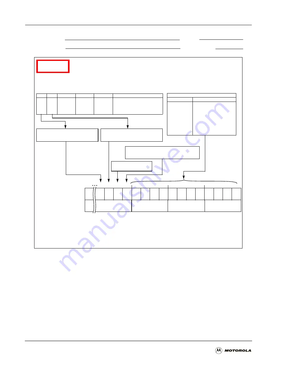
Figure B-19. SCI Clock Control Registers (SCCR)
Application:
Date:
Programmer:
Sheet 2 of 2
SCI
SCI Clock Control Register (SCCR)
15 14 13 12 11 10
9
8
7
6
5
4
3
2
1
0
CD7
CD5
CD4
CD3
CD2
CD1
CD0
23
*
= Reserved, Program as 0
CD6
*
0
TCM RCM
SCP
COD CD11 CD10 CD9
CD8
Clock Divider Bits (CD11–CD0)
CD11–CD0
I
cyc
Rate
$000
I
cyc
/1
$001
I
cyc
/2
$002
I
cyc
/3
•
•
•
•
•
•
$FFE
I
cyc
/4095
$FFF
I
cyc
/4096
SCI Clock Prescaler
0 = ÷1 1 = ÷ 8
Clock Out Divider
0 = Divide clock by 16 before feed to SCLK
1 = Feed clock to directly to SCLK
TCM
RCM
TX Clock
RX Clock
SCLK Pin
Mode
0
0
Internal
Internal
Output
Synchronous/Asynchronous
0
1
Internal
External
Input
Asynchronous only
1
0
External
Internal
Input
Asynchronous only
1
1
External
External
Input
Synchronous/Asynchronous
Receiver Clock Mode/Source
0 = Internal clock for Receiver
1 = External clock from SCLK
Transmitter Clock Mode/Source
0 = Internal clock for Transmitter
1 = External clock from SCLK
Address X:$FFFF9B Read/Write
Reset = $000000
Summary of Contents for DSP56303
Page 1: ...DSP56303 User s Manual 24 Bit Digital Signal Processor DSP56303UM AD Revision 1 January 2001 ...
Page 52: ...JTAG OnCE Interface 2 22 DSP56303 User s Manual ...
Page 114: ...General Purpose Input Output GPIO 5 10 DSP56303 User s Manual ...
Page 212: ...GPIO Signals and Registers 8 26 DSP56303 User s Manual ...
Page 268: ...Interrupt Equates A 22 DSP56303 User s Manual ...
Page 306: ...Programming Sheets B 38 DSP56303 User s Manual ...
Page 320: ...Index 14 DSP56303 User s Manual ...


