


Programming Sheets
B
-32
DSP56303 User’s Manual
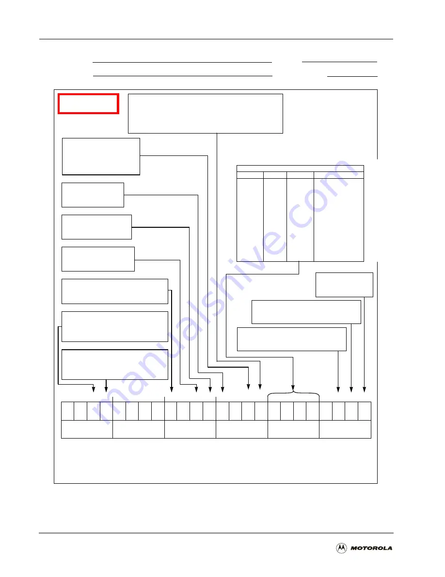
Figure B-21. Timer Control/Status Register (TCSR)
Application:
Date:
Programmer:
Sheet 2 of 3
15 14 13 12 11 10
9
8
7
6
5
4
3
2
1
0
TC3
TC1
TC0
TCIE TQIE
TE
19 18 17 16
23 22 21 20
TCF
TC2
PCE
DO
DI
DIR
TOF
TRM
INV
Timers
*
0
*
0
*
0
*
0
*
0
*
0
*
0
*
0
*
0
Timer Enable Bit 0
0 = Timer Disabled
1 = Timer Enabled
Timer Overflow Interrupt Enable Bit 1
0 = Overflow Interrupts Disabled
1 = Overflow Interrupts Enabled
Inverter Bit 8
0 = 0- to-1 transitions on TIO input increment the counter,
or high pulse width measured, or high pulse output on TIO
1 = 1-to-0 transitions on TIO input increment the counter,
or low pulse width measured, or low pulse output on TIO
Timer Compare Interrupt Enable Bit 2
0 = Compare Interrupts Disabled
1 = Compare Interrupts Enabled
Timer Control/Status Register
TCSR0:$FFFF8F Read/Write
TCSR1:$FFFF8B Read/Write
TCSR2:$FFFF87 Read/Write
Reset = $000000
*
= Reserved, Program as 0
Timer Reload Mode Bit 9
1 = Timer is reloaded when
selected condition occurs
0 = Timer operates as a free
running counter
Timer Overflow Flag Bit 20
0 = “1” has been written to TCSR(TOF),
or timer Overflow interrupt serviced
1 = Counter wraparound has occurred
Direction Bit 11
0 = TIO pin is input
1 = TIO pin is output
Data Output Bit 13
0 = Zero written to TIO pin
1 = One written to TIO pin
Data Input Bit 12
0 = Zero read on TIO pin
1 = One read on TIO pin
Timer Compare Flag Bit 21
0 = “1” has been written to TCSR(TCF),
or timer compare interrupt serviced
1 = Timer Compare has occurred
Prescaled Clock Enable Bit 15
0 = Clock source is CLK/2 or TIO
1 = Clock source is prescaler output
Timer Control Bits 4–7 (TC[3–0])
TC (3:0)
TIO
Clock
Mode
0000
0001
0010
0011
0100
0101
0110
0111
1000
1001
1010
1011
1100
1101
1110
1111
GPIO
Output
Output
Input
Input
Input
Input
Output
–
Output
Output
–
–
–
–
–
Internal
Internal
Internal
External
Internal
Internal
Internal
Internal
–
Internal
Internal
–
–
–
–
–
Timer
Timer Pulse
Timer Toggle
Event Counter
Input Width
Input Period
Capture
Pulse Width Modulation
Reserved
Watchdog Pulse
Watchdog Toggle
Reserved
Reserved
Reserved
Reserved
Reserved
Summary of Contents for DSP56303
Page 1: ...DSP56303 User s Manual 24 Bit Digital Signal Processor DSP56303UM AD Revision 1 January 2001 ...
Page 52: ...JTAG OnCE Interface 2 22 DSP56303 User s Manual ...
Page 114: ...General Purpose Input Output GPIO 5 10 DSP56303 User s Manual ...
Page 212: ...GPIO Signals and Registers 8 26 DSP56303 User s Manual ...
Page 268: ...Interrupt Equates A 22 DSP56303 User s Manual ...
Page 306: ...Programming Sheets B 38 DSP56303 User s Manual ...
Page 320: ...Index 14 DSP56303 User s Manual ...


