


Memory Maps
Memory Configuration
3
-9
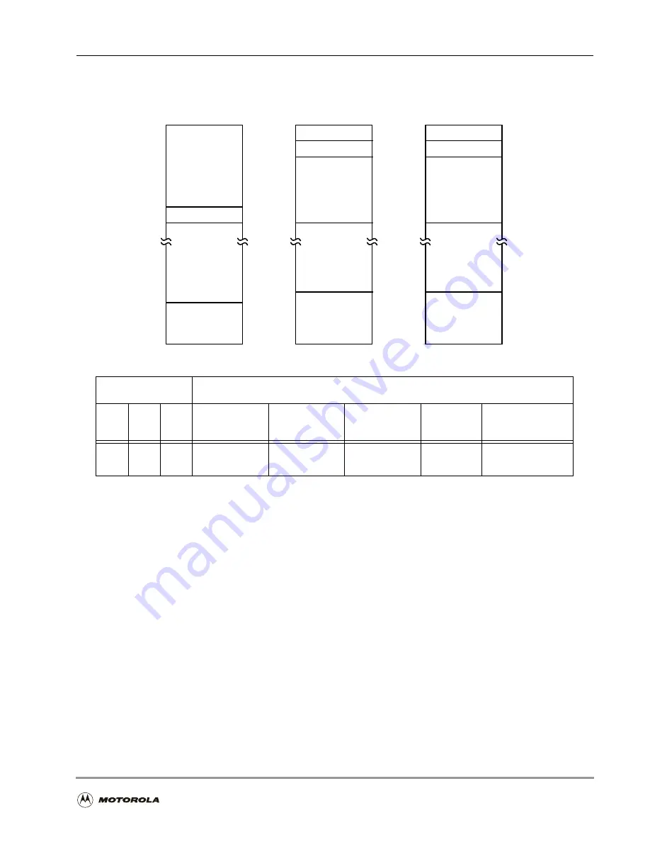
Figure 3-3. Switched Program RAM (0, 1, 0)
Internal
Reserved
Bootstrap ROM
Internal
Program RAM
2 K
$FFFFFF
$FFF0C0
$FF0000
$000000
Internal
Reserved
Internal I/O
External
Internal
X data RAM
3 K
External
$000C00
Internal
Reserved
External I/O
External
Internal
Y data RAM
3 K
External
$FFF000
$FFFF80
Program
X Data
Y Data
Bit Settings
Memory Configuration
SC
MS
CE
Program RAM
X Data RAM
Y Data RAM
Cache
Addressable
Memory Size
0
1
0
2 K
$000–$7FF
3 K
$000–$BFF
3 K
$000–$BFF
None
16 M
External
$FFFFFF
$FF0000
$000000
$000C00
$FFF000
$FFFF80
$FFFFFF
$FF0000
$000000
$000800
Summary of Contents for DSP56303
Page 1: ...DSP56303 User s Manual 24 Bit Digital Signal Processor DSP56303UM AD Revision 1 January 2001 ...
Page 52: ...JTAG OnCE Interface 2 22 DSP56303 User s Manual ...
Page 114: ...General Purpose Input Output GPIO 5 10 DSP56303 User s Manual ...
Page 212: ...GPIO Signals and Registers 8 26 DSP56303 User s Manual ...
Page 268: ...Interrupt Equates A 22 DSP56303 User s Manual ...
Page 306: ...Programming Sheets B 38 DSP56303 User s Manual ...
Page 320: ...Index 14 DSP56303 User s Manual ...


