Bus Interface Unit (BIU) Registers
Core Configuration
4
-25
4.6
Bus Interface Unit (BIU) Registers
The three Bus Interface Unit (BIU) registers configure the external memory expansion port
(Port A). They include the following:
n
Bus Control Register (BCR)
n
DRAM Control Register (DCR)
n
Address Attribute Registers (AAR[3–0])
To use Port A correctly, configure these registers as part of the bootstrap process. The
following subsections describe these registers.
4.6.1
Bus Control Register
The Bus Control Register (BCR), depicted in Figure 4-6, is a read/write register that controls
the external bus activity and Bus Interface Unit (BIU) operation. All BCR bits except bit 21,
BBS, are read/write bits. The BCR bits are defined in Table 4-8.
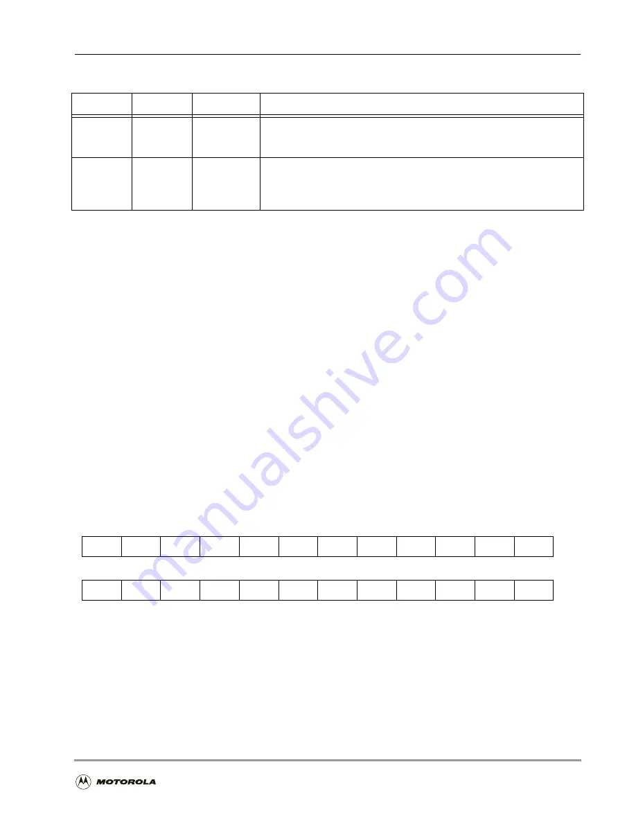
Figure 4-6. Bus Control Register (BCR)
14–12
DF[2–0]
0
Division Factor
Define the DF of the low-power divider. These bits specify the DF as a power
of two in the range from 2
0
to 2
7
.
11–0
MF[11–0]
0
PLL Multiplication Factor
Define the multiplication factor that is applied to the PLL input frequency. The
MF bits are cleared during DSP56303 hardware reset and thus correspond to
an MF of one.
Table 4-7. PLL Control Register (PCTL) Bit Definitions (Continued)
Bit Number
Bit Name
Reset Value
Description
23
22
21
20
19
18
17
16
15
14
13
12
BRH
BLH
BBS
BDFW4 BDFW3 BDFW2 BDFW1 BDFW0 BA3W2 BA3W1 BA3W0 BA2W2
11
10
9
8
7
6
5
4
3
2
1
0
BA2W1 BA2W0 BA1W4 BA1W3 BA1W2 BA1W1 BA1W0 BA0W4 BA0W3 BA0W2 BA0W1 BA0W0
Summary of Contents for DSP56303
Page 1: ...DSP56303 User s Manual 24 Bit Digital Signal Processor DSP56303UM AD Revision 1 January 2001 ...
Page 52: ...JTAG OnCE Interface 2 22 DSP56303 User s Manual ...
Page 114: ...General Purpose Input Output GPIO 5 10 DSP56303 User s Manual ...
Page 212: ...GPIO Signals and Registers 8 26 DSP56303 User s Manual ...
Page 268: ...Interrupt Equates A 22 DSP56303 User s Manual ...
Page 306: ...Programming Sheets B 38 DSP56303 User s Manual ...
Page 320: ...Index 14 DSP56303 User s Manual ...