


Bus Interface Unit (BIU) Registers
4
-30
DSP56303 User’s Manual
4.6.3
Address Attribute Registers (AAR[0–3])
The Address Attribute Registers (AAR[0–3]) are read/write registers that control the activity
of the
AA0
/
RAS0
–
AA3
/
RAS3
pins. The associated
AAn
/
RASn
pin is asserted if the address
defined by the BAC bits in the associated AAR matches the exact number of external address
bits defined by the BNC bits, and the external address space (X data, Y data, or program) is
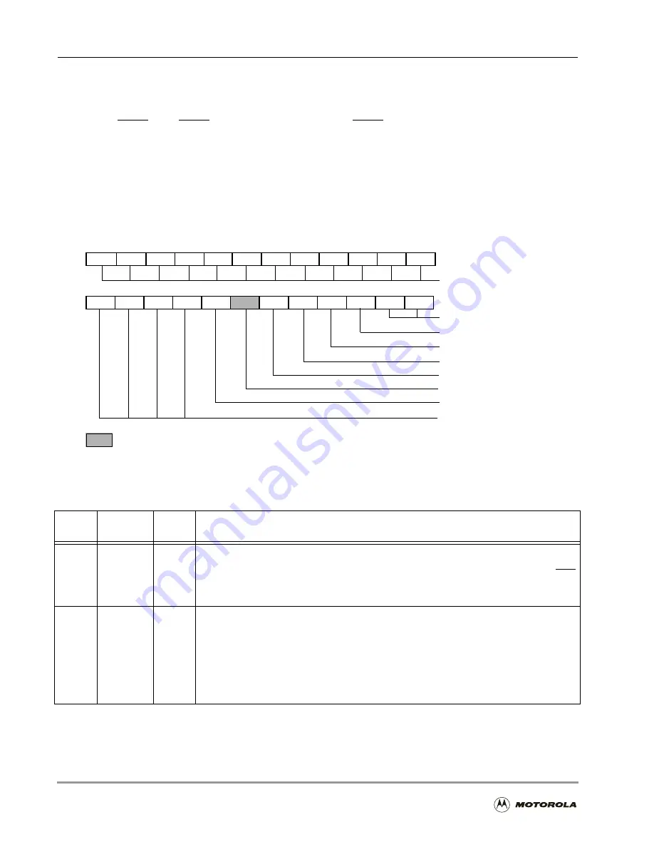
enabled by the AAR. Figure 4-8 shows an AAR register; Table 4-10 lists the bit definitions.
Note:
The DSP56303 does not support address multiplexing.
Figure 4-8. Address Attribute Registers (AAR[0–3]) (X:$FFFFF9–$FFFFF6)
Table 4-10. Address Attribute Registers (AAR[0–3]) Bit Definitions
Bit
Number
Bit Name
Reset
Value
Description
23–12
BAC[11–0]
0
Bus Address to Compare
Read/write control bits that define the upper 12 bits of the 24-bit address with which to
compare the external address to determine whether to assert the corresponding AA/RAS
signal. This is also true of 16-bit compatibility mode. The BNC[3–0] bits define the number
of address bits to compare.
11–8
BNC[3–0]
0
Bus Number of Address Bits to Compare
Specify the number of bits (from the BAC bits) that are compared to the external address.
The BAC bits are always compared with the Most Significant Portion of the external
address (for example, if BNC[3–0] = 0011, then the BAC[11–9] bits are compared to the 3
MSBs of the external address). If no bits are specified (that is, BNC[3–0] = 0000), the AA
signal is activated for the entire 16 M-word space identified by the space enable bits
(BPEN, BXEN, BYEN), but only when the address is external to the internal memory map.
The combinations BNC[3–0] = 1111, 1110, 1101 are reserved.
BAC0
BPEN
0
1
BYEN
2
BAT1
3
BAAP
4
5
6
7
8
9
10
11
BXEN
12
13
14
BAC8
15
16
17
18
19
20
21
22
23
BAT0
BAC3 BAC2
BAC11
BAC5
BAC7 BAC6
BAC9
BAC10
BAC1
BNC3
BNC1
BNC2
BNC0
BAC4
BPAC
Reserved Bit. Write to zero for future compatibility.
External Access Type
AA pin polarity
Program space Enable
X data space Enable
Y data space Enable
Reserved
Packing Enable
Number of Address bit to
compare
Address to Compare
Summary of Contents for DSP56303
Page 1: ...DSP56303 User s Manual 24 Bit Digital Signal Processor DSP56303UM AD Revision 1 January 2001 ...
Page 52: ...JTAG OnCE Interface 2 22 DSP56303 User s Manual ...
Page 114: ...General Purpose Input Output GPIO 5 10 DSP56303 User s Manual ...
Page 212: ...GPIO Signals and Registers 8 26 DSP56303 User s Manual ...
Page 268: ...Interrupt Equates A 22 DSP56303 User s Manual ...
Page 306: ...Programming Sheets B 38 DSP56303 User s Manual ...
Page 320: ...Index 14 DSP56303 User s Manual ...


