On-Chip Emulation Module
Introduction
MOTOROLA
DSP56309UM/D 10-3
10.1
INTRODUCTION
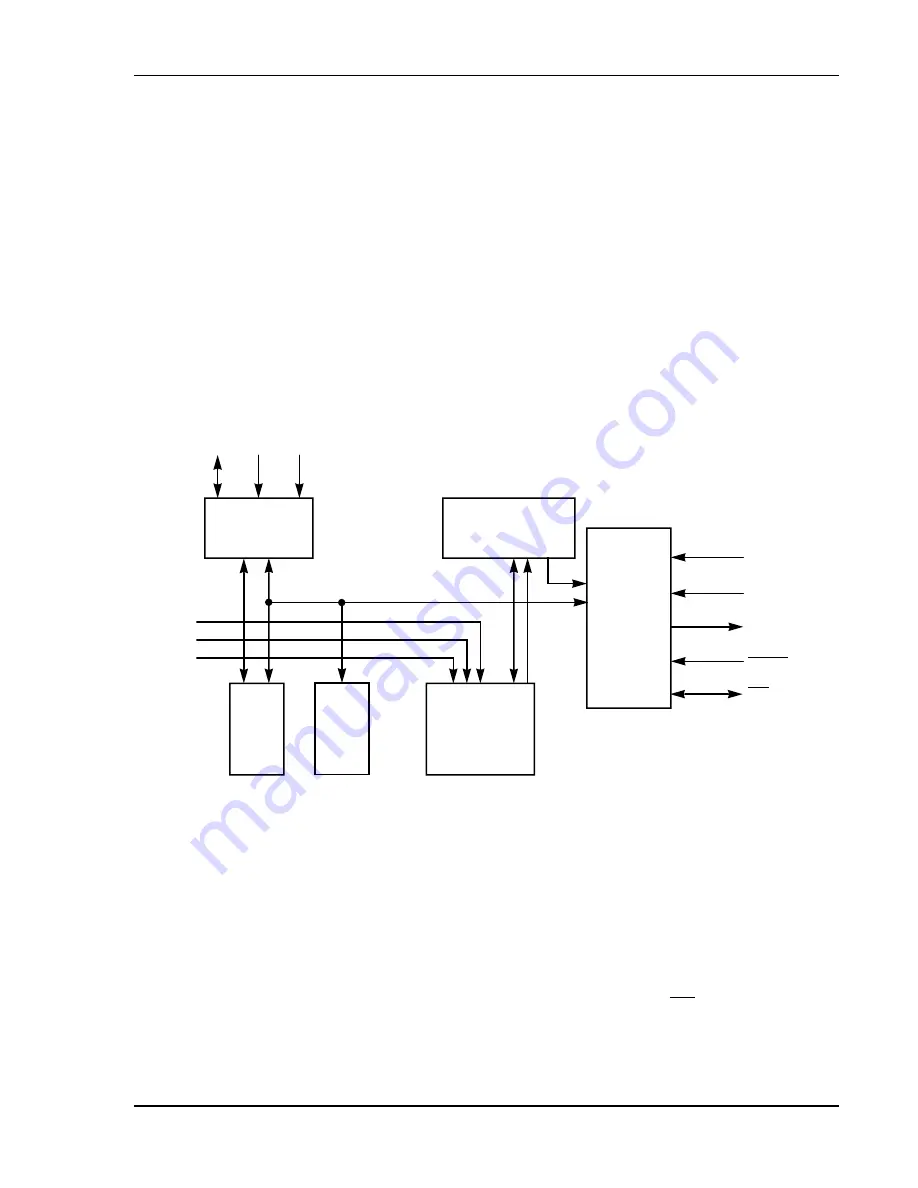
The DSP56300 core On-Chip Emulation (OnCEª) module provides a means of
interacting with the DSP56300 core and its peripherals nonintrusively so that a user can
examine registers, memory, or on-chip peripherals, thus facilitating hardware and
software development on the DSP56300 core processor. To achieve this, special circuits
and dedicated signals on the DSP56300 core are defined to avoid sacrificing any
user-accessible on-chip resource. The OnCE module resources can be accessed only after
executing the JTAG instruction ENABLE_ONCE. These resources are accessible even
when the chip is operating in normal mode. See
of the JTAG functionality and its relation to the OnCE module.
block diagram of the OnCE module.
10.2
OnCE MODULE SIGNALS
The OnCE module controller functionality is accessed through the JTAG port. There are
no dedicated OnCE module signals for the clock, data in, or data out. The JTAG signals
TCK, TDI, and TDO are used to shift in and out data and instructions. See
on page 11-4 for the description of the JTAG signals. To
facilitate emulation-specific functions, one additional signal, called DE, is provided on
the DSP56309.
Figure 10-1
OnCE Module Block Diagram
Trace
Buffer
Breakpoint
Logic
Pipeline
Information
Trace Logic
OnCE
Controller
PAB
YAB
XAB
PDB
PIL GDB
TDO
TRST
TDI
TCK
Tags
Buffer
Control Bus
DE
AA0702
Summary of Contents for DSP56309
Page 25: ...xxii DSP56309UM D MOTOROLA Figure D 25 Port E Registers PCRE PRRE PDRE D 39 ...
Page 30: ...MOTOROLA DSP56309UM D 1 1 SECTION 1 DSP56309 OVERVIEW ...
Page 47: ...1 18 DSP56309UM D MOTOROLA DSP56309 Overview DSP56309 Architecture Overview ...
Page 48: ...MOTOROLA DSP56309UM D 2 1 SECTION 2 SIGNAL CONNECTION DESCRIPTIONS ...
Page 85: ...2 38 DSP56309UM D MOTOROLA Signal Connection Descriptions OnCE JTAG Interface ...
Page 86: ...MOTOROLA DSP56309UM D 3 1 SECTION 3 MEMORY CONFIGURATION ...
Page 104: ...MOTOROLA DSP56309UM D 4 1 SECTION 4 CORE CONFIGURATION ...
Page 124: ...MOTOROLA DSP56309UM D 5 1 SECTION 5 GENERAL PURPOSE I O ...
Page 125: ...5 2 DSP56309UM D MOTOROLA General Purpose I O 5 1 INTRODUCTION 5 3 5 2 PROGRAMMING MODEL 5 3 ...
Page 128: ...MOTOROLA DSP56309UM D 6 1 SECTION 6 HOST INTERFACE HI08 ...
Page 166: ...MOTOROLA DSP56309UM D 7 1 SECTION 7 ENHANCED SYNCHRONOUS SERIAL INTERFACE ESSI ...
Page 212: ...MOTOROLA DSP56309UM D 8 1 SECTION 8 SERIAL COMMUNICATION INTERFACE SCI ...
Page 241: ...8 30 DSP56309UM D MOTOROLA Serial Communication Interface SCI GPIO Signals and Registers ...
Page 242: ...MOTOROLA DSP56309UM D 9 1 SECTION 9 TRIPLE TIMER MODULE ...
Page 269: ...9 28 DSP56309UM D MOTOROLA Triple Timer Module Timer Operational Modes ...
Page 270: ...MOTOROLA DSP56309UM D 10 1 SECTION 10 ON CHIP EMULATION MODULE ...
Page 302: ...MOTOROLA DSP56309UM D 11 1 SECTION 11 JTAG PORT ...
Page 369: ...C 22 DSP56309UM D MOTOROLA DSP56309 BSDL Listing ...
Page 370: ...MOTOROLA DSP56309UM D D 1 APPENDIX D PROGRAMMING REFERENCE ...
Page 405: ......
Page 409: ......


