10-28
DSP56367
MOTOROLA
Enhanced Serial Audio Interface (ESAI)
ESAI Programming Model
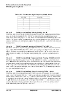
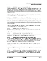
10.3.3.7
RCCR Receiver High Frequency Clock Polarity (RHCKP) - Bit 20
The Receiver High Frequency Clock Polarity (RHCKP) bit controls on which bit clock edge
data and frame sync are clocked out and latched in. If RHCKP is cleared the data and the
frame sync are clocked out on the rising edge of the receive bit clock and the frame sync is
latched in on the falling edge of the receive bit clock. If RHCKP is set the falling edge of the
receive clock is used to clock the data and frame sync out and the rising edge of the receive
clock is used to latch the frame sync in.
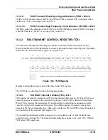
10.3.3.8
RCCR Receiver Clock Source Direction (RCKD) - Bit 21
The Receiver Clock Source Direction (RCKD) bit selects the source of the clock signal used
to clock the receive shift register in the asynchronous mode (SYN=0) and the IF0/OF0 flag
direction in the synchronous mode (SYN=1).
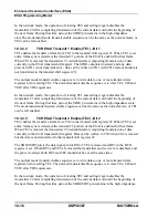
In the asynchronous mode when RCKD is set, the internal clock source becomes the bit clock
for the receive shift registers and word length divider, and is the output on the SCKR pin. In
the asynchronous mode when RCKD is cleared, the clock source is external; the internal clock
generator is disconnected from the SCKR pin, and an external clock source may drive this pin.
In the synchronous mode when RCKD is set, the SCKR pin becomes the OF0 output flag. If
RCKD is cleared, then the SCKR pin becomes the IF0 input flag. See Table 10-1 and
Table 10-7.
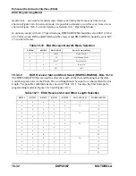
10.3.3.9
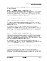
RCCR Receiver Frame Sync Signal Direction (RFSD) - Bit 22
The Receiver Frame Sync Signal Direction (RFSD) bit selects the source of the receiver frame
sync signal when in the asynchronous mode (SYN=0), and the IF1/OF1/Transmitter Buffer
Enable flag direction in the synchronous mode (SYN=1).
In the asynchronous mode when RFSD is set, the internal clock generator becomes the source
of the receiver frame sync, and is the output on the FSR pin. In the asynchronous mode when
RFSD is cleared, the receiver frame sync source is external; the internal clock generator is
disconnected from the FSR pin, and an external clock source may drive this pin.
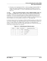
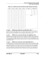
Table 10-7 SCKR Pin Definition Table
Control Bits
SCKR PIN
SYN
RCKD
0
0
SCKR input
0
1
SCKR output
1
0
IF0
1
1
OF0
Summary of Contents for DSP56367
Page 16: ...xvi MOTOROLA CONTENTS Paragraph Number Title Page Number ...
Page 22: ...xxii MOTOROLA List of Figures Figure Number Title Page Number ...
Page 26: ...xxvi MOTOROLA List of Tables Table Number Title Page Number ...
Page 148: ...4 6 DSP56367 MOTOROLA Design Considerations PLL Performance Issues ...
Page 248: ...9 30 DSP56367 MOTOROLA Serial Host Interface SHI Programming Considerations ...
Page 306: ...10 58 DSP56367 MOTOROLA Enhanced Serial Audio Interface ESAI ESAI Initialization Examples ...
Page 389: ...Bootstrap ROM Contents MOTOROLA DSP56367 A 15 end ...
Page 390: ...A 16 DSP56367 MOTOROLA Bootstrap ROM Contents ...
Page 432: ...C 8 DSP56367 MOTOROLA JTAG BSDL ...
Page 484: ...D 52 DSP56367 MOTOROLA Programmer s Reference ...
Page 490: ...E 6 DSP56367 MOTOROLA Power Consumption Benchmark ...
Page 516: ...F 26 DSP56367 MOTOROLA IBIS Model ...
Page 522: ...Index 6 MOTOROLA Index ...
Page 523: ......

