7 - 48
DSP96002 USER’S MANUAL
MOTOROLA
the DMA transfer. If an input is unmasked, asserting that input will set the latch and initiate a DMA transfer.
The DMA state machine clears the latch when accessing the DMA source address. If more than one re-
questing device input is enabled, the first edge on any input is latched and triggers a DMA transfer, and any
other edge that appears before the latch is cleared will be ignored.
7.5.3.5
DCS DMA Channel Priority (DCP) Bit 23
The DMA Channel Priority (DCP) bit contains the priority level of the DMA channel relative to the other DMA
channel. When DMA transfers are pending, the DMA Channel Priority of both channels are compared to
decide which channel will be activated. This decision must be made since both channels use common re-
sources such as the DMA ALU, and the address buses. DCP is cleared by Hardware and Software Reset.
If both channels have the same priority then the channels will be active in a round-robin fashion: Channel 0
will be activated to transfer a single data word, followed by Channel 1.
If the channel priorities are different, the channel with highest priority will start executing DMA transfers and
will remain doing so as long as there are DMA transfers pending. In the event that the lower priority channel
is executing DMA transfers when the higher priority channel receives a transfer request, the lower priority
channel will finish the transfer of the current data word and arbitration will again occur.
7.5.3.6
DCS DMA Priority (DMAP) Bit 24
This bit permits setting the DMA priority relative to the core when an external bus access is required. The
priority determines, in case of contention between the core and the DMA Controller, whether the DMA will
wait or not. If DMAP is cleared, then the DMA will wait until a free slot is available on the external bus. If
DMAP is set, the core cycle will be stretched and both core and DMA will access during the same cycle.
DMAP is cleared by Hardware and Software Reset.
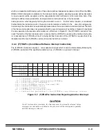
DMA Request
Mask BitRequesting Device
M0 External (
–
I
—
R
—
Q
–
A pin)
M1 External (
–
I
—
R
—
Q
–
B pin)
M2 External (
–
I
—
R
—
Q
–
C pin)
M3 Port A Host Receive Data (HRDF=1)
M4 Port A Host Transmit Data (HTXE=1)
M5 Port B Host Receive Data (HRDF=1)
M6 Port B Host Transmit Data (HTXE=1)
DCP
DMA Channel Priority
0 Priority 0
1 Priority 1
DMAP
External Access Priority
0 Core
1 Equal
Summary of Contents for DSP96002
Page 3: ...1 2 DSP96002 USER S MANUAL MOTOROLA ...
Page 38: ...MOTOROLA DSP96002 USER S MANUAL 3 15 Figure 3 4 Modulo Arithmetic Unit Block Diagram ...
Page 39: ...3 16 DSP96002 USER S MANUAL MOTOROLA ...
Page 53: ...4 14 DSP96002 USER S MANUAL MOTOROLA ...
Page 76: ...MOTOROLA DSP96002 USER S MANUAL 5 23 Figure 5 8 Address Modifier Summary ...
Page 86: ...6 10 DSP96002 USER S MANUAL MOTOROLA ...
Page 101: ...MOTOROLA DSP96002 USER S MANUAL 7 15 Figure 7 9 HI Block Diagram One Port ...
Page 140: ...7 54 DSP96002 USER S MANUAL MOTOROLA ...
Page 166: ...9 10 DSP96002 USER S MANUAL MOTOROLA ...
Page 181: ...MOTOROLA DSP96002 USER S MANUAL 10 15 Figure 10 8 Program Address Bus FIFO ...
Page 337: ...MOTOROLA DSP96002 USER S MANUAL A 149 ...
Page 404: ...A 216 DSP96002 USER S MANUAL MOTOROLA PC xxxx D ...
Page 460: ...A 272 DSP96002 USER S MANUAL MOTOROLA SIOP Not affected ...
Page 484: ...A 296 DSP96002 USER S MANUAL MOTOROLA SSH PC SSL SR SP 1 SP ...
Page 519: ...MOTOROLA DSP96002 USER S MANUAL A 331 ...
Page 718: ...MOTOROLA DSP96002 USER S MANUAL B 199 ...
Page 871: ... MOTOROLA INC 1994 MOTOROLA TECHNICAL DATA SEMICONDUCTOR M Addendum ...
Page 888: ...MOTOROLA INDEX 1 INDEX ...
Page 889: ......


