MOTOROLA
DSP96002 USER’S MANUAL
10 - 1
SECTION 10
ON-CHIP EMULATOR
10.1
INTRODUCTION
Conventional methods of system development (for example the DSP56001) consist of a program which re-
sides in the DSP program memory (monitor). An interface circuit which either uses on-chip resources or an
additional program memory address communicates with a host computer or terminal. This technique is not
transparent, loads the DSP bus and sometimes interferes with the user system configuration. To emulate
the DSP in a user’s target system an expensive cable must be used to bring out the DSP pins onto the sys-
tem under development.
The DSP96002’s on-chip emulation (OnCE
) circuitry provides a means of interacting with the DSP96002
and its peripherals non-intrusively so that a user may examine registers, memory or on-chip peripherals.
This will facilitate hardware/software development on the DSP96002 processor. To achieve this, special cir-
cuits and dedicated pins on the DSP96002 die are defined to avoid sacrificing any user accessible on-chip
resource.
A key feature of the OnCE
dedicated pins is to allow the user to insert the DSP96002 into his target system
yet retaining debug control. The need for a costly cable which brings out the DSP96002 footprint on an em-
ulator system is eliminated because of the easy access to the dedicated OnCE
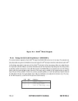
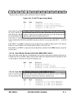
debug serial port. Figure
10-1illustrates the block diagram of the OnCE
serial interface.
10.2
ON-CHIP EMULATION (OnCE
) PINOUT
10.2.1
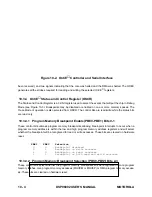
Debug Serial Input/Chip Status 0 (DSI/OS0)
Serial data or commands are provided to the OnCE
controller through the DSI/OS0 pin when it is an input.
The data received on the DSI pin will be recognized only when the DSP96002 has entered the debug mode
of operation. Data must have valid TTL logic levels before being latched on the falling edge of the serial
clock. Data is always shifted into the OnCE
serial port most significant bit (MSB) first. When an output,
this pin in conjunction with the OS1 pin, provides information about the chip status indicating why the debug
mode cannot be entered in response to an external request. The DSI/OS0 pin is an output when not in De-
bug Mode (until the acknowledge signal is issued to the Command Controller). When switching from output
to input, the pin is three-stated. In order to avoid any possible glitches, an external pull-down resistor should
be attached to this pin. During hardware reset, this pin is defined as an output and it is driven low.
OnCE
is a trademark of Motorola Inc.
Summary of Contents for DSP96002
Page 3: ...1 2 DSP96002 USER S MANUAL MOTOROLA ...
Page 38: ...MOTOROLA DSP96002 USER S MANUAL 3 15 Figure 3 4 Modulo Arithmetic Unit Block Diagram ...
Page 39: ...3 16 DSP96002 USER S MANUAL MOTOROLA ...
Page 53: ...4 14 DSP96002 USER S MANUAL MOTOROLA ...
Page 76: ...MOTOROLA DSP96002 USER S MANUAL 5 23 Figure 5 8 Address Modifier Summary ...
Page 86: ...6 10 DSP96002 USER S MANUAL MOTOROLA ...
Page 101: ...MOTOROLA DSP96002 USER S MANUAL 7 15 Figure 7 9 HI Block Diagram One Port ...
Page 140: ...7 54 DSP96002 USER S MANUAL MOTOROLA ...
Page 166: ...9 10 DSP96002 USER S MANUAL MOTOROLA ...
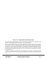
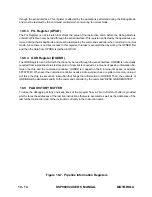
Page 181: ...MOTOROLA DSP96002 USER S MANUAL 10 15 Figure 10 8 Program Address Bus FIFO ...
Page 337: ...MOTOROLA DSP96002 USER S MANUAL A 149 ...
Page 404: ...A 216 DSP96002 USER S MANUAL MOTOROLA PC xxxx D ...
Page 460: ...A 272 DSP96002 USER S MANUAL MOTOROLA SIOP Not affected ...
Page 484: ...A 296 DSP96002 USER S MANUAL MOTOROLA SSH PC SSL SR SP 1 SP ...
Page 519: ...MOTOROLA DSP96002 USER S MANUAL A 331 ...
Page 718: ...MOTOROLA DSP96002 USER S MANUAL B 199 ...
Page 871: ... MOTOROLA INC 1994 MOTOROLA TECHNICAL DATA SEMICONDUCTOR M Addendum ...
Page 888: ...MOTOROLA INDEX 1 INDEX ...
Page 889: ......

