MOTOROLA
DSP96002 USER’S MANUAL
10 - 3
10.2.3
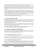
Debug Serial Output (DSO)
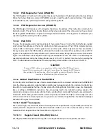
The debug serial output provides the data contained in one of the OnCE
controller registers as specified
by the last command received from the external command controller. When idle, this pin is held high. When
the requested data is available, the DSO line will be asserted (negative true logic) for two T cycles (2T =
period of DSP96002 master clock) to indicate that the serial shift registers are ready to receive clocks in
order to deliver the data. When a trace or breakpoint occurs this line will be asserted for one T cycle to
indicate (acknowledge) that the chip has entered the debug mode and is waiting for commands. Data is
always shifted out the OnCE
serial port most significant bit (MSB) first. During hardware reset, this pin is
held high.
10.2.4
Debug Enable Input (
—
D
–
R)
The debug request input provides a means of entering the debug mode of operation from the external com-
mand controller. This pin, when asserted, causes the DSP96002 to finish the current instruction being exe-
cuted, save the instruction pipeline information, enter the debug mode, and wait for commands to be en-
tered from the debug serial input line.
10.3
OnCE
CONTROLLER AND SERIAL INTERFACE
The OnCE
Controller and Serial Interface contains the following blocks: input shift register, bit counter,
OnCE
decoder, and the status/control register. Figure 10-2 illustrates a block diagram of the OnCE
se-
rial interface.
10.3.1
OnCE
Input Shift Register (OISR)
The OnCE
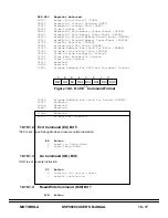
Input Shift Register is an 8-bit shift register that receives the serial data from the DSI line. The
data is clocked into the register on the falling edge of the clock applied to the DSCK pin. After the 8th bit is
received, the OISR will stop shifting in new data. The latched data will be used as input for the OnCE
De-
coder. The data is always shifted into the OISR most significant bit (MSB) first.
10.3.2
OnCE
Bit Counter (OBC)
The OnCE
Bit Counter is a 5-bit counter associated with shifting in and out the data bits. The OBC is in-
cremented by the falling edges of the DSCK. The OBC is cleared during hardware reset and whenever the
DSP96002 acknowledges that the Debug Mode has been entered. The OBC supplies two signals to the
OnCE
Decoder: one indicating that the first 8 bits were shifted-in (so a new command is available) and
the second indicating that 32 bits were shifted-in (the data associated with that command is available) or
that 32 bits were shifted-out (the data required by a read command was shifted out).
10.3.3
OnCE
Decoder (ODEC)
The OnCE
Decoder supervises the entire OnCE
activity. It receives as input the 8-bit command from the
OISR, two signals from OBC (one indicating that 8 bits have been received and the other that 32 bits have
Summary of Contents for DSP96002
Page 3: ...1 2 DSP96002 USER S MANUAL MOTOROLA ...
Page 38: ...MOTOROLA DSP96002 USER S MANUAL 3 15 Figure 3 4 Modulo Arithmetic Unit Block Diagram ...
Page 39: ...3 16 DSP96002 USER S MANUAL MOTOROLA ...
Page 53: ...4 14 DSP96002 USER S MANUAL MOTOROLA ...
Page 76: ...MOTOROLA DSP96002 USER S MANUAL 5 23 Figure 5 8 Address Modifier Summary ...
Page 86: ...6 10 DSP96002 USER S MANUAL MOTOROLA ...
Page 101: ...MOTOROLA DSP96002 USER S MANUAL 7 15 Figure 7 9 HI Block Diagram One Port ...
Page 140: ...7 54 DSP96002 USER S MANUAL MOTOROLA ...
Page 166: ...9 10 DSP96002 USER S MANUAL MOTOROLA ...
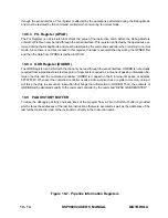
Page 181: ...MOTOROLA DSP96002 USER S MANUAL 10 15 Figure 10 8 Program Address Bus FIFO ...
Page 337: ...MOTOROLA DSP96002 USER S MANUAL A 149 ...
Page 404: ...A 216 DSP96002 USER S MANUAL MOTOROLA PC xxxx D ...
Page 460: ...A 272 DSP96002 USER S MANUAL MOTOROLA SIOP Not affected ...
Page 484: ...A 296 DSP96002 USER S MANUAL MOTOROLA SSH PC SSL SR SP 1 SP ...
Page 519: ...MOTOROLA DSP96002 USER S MANUAL A 331 ...
Page 718: ...MOTOROLA DSP96002 USER S MANUAL B 199 ...
Page 871: ... MOTOROLA INC 1994 MOTOROLA TECHNICAL DATA SEMICONDUCTOR M Addendum ...
Page 888: ...MOTOROLA INDEX 1 INDEX ...
Page 889: ......

