MOTOROLA
DSP96002 USER’S MANUAL
7 - 1
SECTION 7
EXPANSION PORTS AND I/O PERIPHERALS
7.1
INTRODUCTION
The upper 128 locations of the X and Y Data memories are defined as the I/O space. The Y memory I/O
space is wholly external, while the X memory I/O space is internal. The X memory I/O space is used to ad-
dress the I/O Interface registers as well as the bus, port select and interrupt control registers. Both I/O spac-
es may be accessed by regular X and Y memory MOVE instructions. The MOVEP instructions offer I/O
short addressing and memory to memory move capability for easy data transfers with the I/O mapped reg-
isters.
The on-chip I/O peripherals are intended to minimize system chip count and "glue" logic in many applica-
tions. Each I/O interface has its own control, status and data registers memory-mapped into the X memory
I/O space. Each interface has several dedicated interrupt vector addresses and control bits to enable/dis-
able interrupts. This minimizes the overhead associated with servicing the device since each interrupt
source has its own service routine.
Three on-chip peripherals are provided in the DSP96002:
•
a 32-bit parallel Host MPU/DMA Interface connected to Port A.
•
a 32-bit parallel Host MPU/DMA Interface connected to Port B.
•
a two-channel DMA Controller.
7.2
EXPANSION PORTS CONTROL
The DSP96002 has two external expansion ports (Port A and Port B). Each port has a bus control register
where memory wait states may be specified, parameter and control bits for a page circuit dedicated to
DRAM/VRAM memory support are located, and control bits for direct software control of
—
B
–
R and
—
B
–
L pins are found.
7.2.1 Bus Control Registers (BCRA and BCRB)
There are 2 identical BCR registers, one for each port. The Bus Control Registers (BCRx) may be pro-
grammed to insert wait states in a bus cycle during external memory accesses. They are also used to pro-
gram the Page Fault circuitry and for direct software control of the
—
B
–
R and
—
B
–
L pins.
Summary of Contents for DSP96002
Page 3: ...1 2 DSP96002 USER S MANUAL MOTOROLA ...
Page 38: ...MOTOROLA DSP96002 USER S MANUAL 3 15 Figure 3 4 Modulo Arithmetic Unit Block Diagram ...
Page 39: ...3 16 DSP96002 USER S MANUAL MOTOROLA ...
Page 53: ...4 14 DSP96002 USER S MANUAL MOTOROLA ...
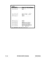
Page 76: ...MOTOROLA DSP96002 USER S MANUAL 5 23 Figure 5 8 Address Modifier Summary ...
Page 86: ...6 10 DSP96002 USER S MANUAL MOTOROLA ...
Page 101: ...MOTOROLA DSP96002 USER S MANUAL 7 15 Figure 7 9 HI Block Diagram One Port ...
Page 140: ...7 54 DSP96002 USER S MANUAL MOTOROLA ...
Page 166: ...9 10 DSP96002 USER S MANUAL MOTOROLA ...
Page 181: ...MOTOROLA DSP96002 USER S MANUAL 10 15 Figure 10 8 Program Address Bus FIFO ...
Page 337: ...MOTOROLA DSP96002 USER S MANUAL A 149 ...
Page 404: ...A 216 DSP96002 USER S MANUAL MOTOROLA PC xxxx D ...
Page 460: ...A 272 DSP96002 USER S MANUAL MOTOROLA SIOP Not affected ...
Page 484: ...A 296 DSP96002 USER S MANUAL MOTOROLA SSH PC SSL SR SP 1 SP ...
Page 519: ...MOTOROLA DSP96002 USER S MANUAL A 331 ...
Page 718: ...MOTOROLA DSP96002 USER S MANUAL B 199 ...
Page 871: ... MOTOROLA INC 1994 MOTOROLA TECHNICAL DATA SEMICONDUCTOR M Addendum ...
Page 888: ...MOTOROLA INDEX 1 INDEX ...
Page 889: ......

