7 - 4
DSP96002 USER’S MANUAL
MOTOROLA
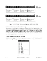
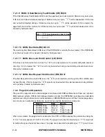
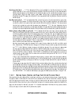
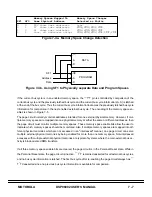
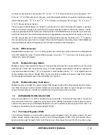
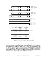
7.2.1.9 BCRx X Data Memory Fault Enable (XE) Bit 28
If the X Data Memory Fault Enable bit XE is set, the page fault circuit will monitor X Data memory bus cycles.
If XE is set and a fault is detected during a X Data memory bus cycle,
—
T
–
T will be deasserted. If XE is set
and no fault is detected during a X Data memory bus cycle,
—
T
–
T will be asserted. If XE is cleared, the
page fault circuit will be inactive for X Data memory bus cycles and
—
T
–
T will remain deasserted. XE is
cleared by hardware reset.
7.2.1.10 BCRx Bus State (BS) Bit 29
The read-only Bus State status bit BS is set if the DSP96002 is currently the bus master. If the DSP96002
is not the bus master, BS is cleared. Cleared by hardware reset.
7.2.1.11 BCRx Bus Lock Hold Control (LH) Bit 30
If the Bus Lock Hold control bit LH is set, the
—
B
–
L pin is asserted even if no read-modify-write access is
occurring. If LH is cleared, the
—
B
–
L pin will only be asserted during a read-modify-write external access.
Cleared by hardware reset.
7.2.1.12 BCRx Bus Request Hold Control (RH) Bit 31
If the Bus Request Hold control bit RH is set, the
—
B
–
R pin is asserted even though the CPU or DMA does
not need the bus. If RH is cleared, the
—
B
–
R pin will only be asserted if an external access is being attempt-
ed or pending. Cleared by hardware reset.
7.2.2 Page Circuit Operation
The goal of the page circuit is to allow designers to achieve static RAM performance with low cost, dynamic
RAM memory systems. With its internal page detection circuitry, the DSP96002 can achieve zero wait state
performance using the fast access modes available on DRAM/VRAM devices. Without internal page detec-
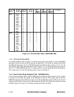
tion circuitry, zero wait state performance would not be possible. Example memories are:
When a bus master, the page circuit is active when the CPU or DMA accesses the external bus using the
P, X or Y memory spaces (S1:S0=10, 01 or 00). The page circuit uses the transfer type (
—
T
–
T) output pin
to indicate the type of external bus access. The page circuit asserts the transfer type (
—
T
–
T) pin when an
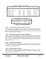
XE
—
T
–
T Pin Activity for X Space
0 Deasserted
1 Active
Device
Size
Mode
MCM514256A
256K x 4
Page
MCM51L1000A
1Meg x 1
Page
MCM514258A
256K x 4
Static Column
MCM511002A
1Meg x 1
Static Column
Summary of Contents for DSP96002
Page 3: ...1 2 DSP96002 USER S MANUAL MOTOROLA ...
Page 38: ...MOTOROLA DSP96002 USER S MANUAL 3 15 Figure 3 4 Modulo Arithmetic Unit Block Diagram ...
Page 39: ...3 16 DSP96002 USER S MANUAL MOTOROLA ...
Page 53: ...4 14 DSP96002 USER S MANUAL MOTOROLA ...
Page 76: ...MOTOROLA DSP96002 USER S MANUAL 5 23 Figure 5 8 Address Modifier Summary ...
Page 86: ...6 10 DSP96002 USER S MANUAL MOTOROLA ...
Page 101: ...MOTOROLA DSP96002 USER S MANUAL 7 15 Figure 7 9 HI Block Diagram One Port ...
Page 140: ...7 54 DSP96002 USER S MANUAL MOTOROLA ...
Page 166: ...9 10 DSP96002 USER S MANUAL MOTOROLA ...
Page 181: ...MOTOROLA DSP96002 USER S MANUAL 10 15 Figure 10 8 Program Address Bus FIFO ...
Page 337: ...MOTOROLA DSP96002 USER S MANUAL A 149 ...
Page 404: ...A 216 DSP96002 USER S MANUAL MOTOROLA PC xxxx D ...
Page 460: ...A 272 DSP96002 USER S MANUAL MOTOROLA SIOP Not affected ...
Page 484: ...A 296 DSP96002 USER S MANUAL MOTOROLA SSH PC SSL SR SP 1 SP ...
Page 519: ...MOTOROLA DSP96002 USER S MANUAL A 331 ...
Page 718: ...MOTOROLA DSP96002 USER S MANUAL B 199 ...
Page 871: ... MOTOROLA INC 1994 MOTOROLA TECHNICAL DATA SEMICONDUCTOR M Addendum ...
Page 888: ...MOTOROLA INDEX 1 INDEX ...
Page 889: ......


