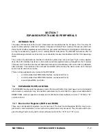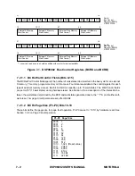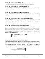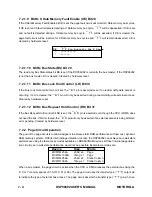
7 - 6
DSP96002 USER’S MANUAL
MOTOROLA
Non-Sequential Fault
-
—
T
–
T is deasserted if the current address A is not the increment (+1) of the
latched address A’. The non-sequential fault is enabled if the NS control bit is set, otherwise disabled.
Nibble mode accesses on the random port or serial accesses on the serial port can cause non-se-
quential faults. Page and static column mode RAMs cannot have non-sequential faults and NS
should be cleared. The page circuit checks for non-sequential faults for addresses that are inside the
defined page.
Bus Mastership Fault
-
—
T
–
T is deasserted if the current bus cycle is the first external bus cycle since
becoming the bus master. The first external bus cycle by any bus master typically is not a fast access
mode since other bus masters may have accessed the same external memory. This also ensures
that the first external bus cycle after hardware reset deasserts
—
T
–
T. The bus mastership fault is
enabled if the MF control bit is set, otherwise disabled. It is possible that certain multiple processor
systems may want to disable this feature if the external memory is allocated to a particular processor.
Memory Space (Physical Memory) Faults
-
—
T
–
T is deasserted if the current bus cycle accesses a dif-
ferent memory space than the previously latched bus cycle. This is useful if the space select pins S1
or S0 are used as address lines to the external memory. In this case, the user is mapping the same
address in different memory spaces to DIFFERENT physical memory locations. If the space select
pins S1 and S0 are not being used as address lines to the external memory, the user is mapping the
same address in different memory spaces to the SAME physical memory location so changes in
memory space should be ignored. This is an example of the "single memory space" mentality prev-
alent in systems executing high level languages like C.
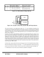
Memory space faults based on changes in S1 and/or S0 are enabled by the SF1 and SF0 control
bits, respectively. If SF1(SF0) is set, changes in S1(S0) will cause a memory space fault and deas-
sert
—
T
–
T. If SF1(SF0) is cleared, changes in S1(S0) are ignored. The user memory mapping and
memory space change detection for each SF1 and SF0 combination are given in Figure 7-4a.
Note that both the current bus cycle C and the previously latched bus cycle C’ represent accesses
to one of the three memory spaces. The S1:S0=11 combination will never appear as a current or
latched memory space value, since it means that no access is being done (S1:S0 = 00
⇒
Y, S1:S0
= 01
⇒
X, S1:S0 = 10
⇒
P).
There is one combination (PX) missing from this encoding - where P and X share the same address-
es. Since this combination cannot directly use S1 or S0 as address lines, its use will not be as popular
and its implementation would require control on a "per-space" basis instead of the "per-pin" basis as
shown above.
This discussion assumes that if S1 and/or S0 are used as address lines, they are introduced as high
order address lines above the page size boundary. If S1 and/or S0 are introduced as low order ad-
dresses below the page size boundary, proper page fault operation can be achieved by adjusting the
page size but the non-sequential fault detection cannot be used. Therefore, it is recommended that
S1 and S0 only be used as high order address lines above the page size boundary. An example sys-
tem with SF1:SF0 = 10 to detect shifts between program and data spaces is shown in Figure 7-4b.
7.2.2.1
Memory Space Enables and Page Fault Circuit Personal Reset
The page fault circuit is enabled if the current bus cycle is in a user selected memory space. Separate mem-
ory space enable control bits (PE, XE and YE) are provided so the user can select the memory space(s)
which the page fault circuit monitors. If a memory space enable bit (PE, XE and/or YE) is set, the page fault
circuit is active if the current bus cycle is in that memory space. If a memory space enable bit is cleared, the
page circuit is inactive for that bus cycle and
—
T
–
T remains deasserted. If all three memory space enables
are set, the page circuit is active for all external bus cycles.
Summary of Contents for DSP96002
Page 3: ...1 2 DSP96002 USER S MANUAL MOTOROLA ...
Page 38: ...MOTOROLA DSP96002 USER S MANUAL 3 15 Figure 3 4 Modulo Arithmetic Unit Block Diagram ...
Page 39: ...3 16 DSP96002 USER S MANUAL MOTOROLA ...
Page 53: ...4 14 DSP96002 USER S MANUAL MOTOROLA ...
Page 76: ...MOTOROLA DSP96002 USER S MANUAL 5 23 Figure 5 8 Address Modifier Summary ...
Page 86: ...6 10 DSP96002 USER S MANUAL MOTOROLA ...
Page 101: ...MOTOROLA DSP96002 USER S MANUAL 7 15 Figure 7 9 HI Block Diagram One Port ...
Page 140: ...7 54 DSP96002 USER S MANUAL MOTOROLA ...
Page 166: ...9 10 DSP96002 USER S MANUAL MOTOROLA ...
Page 181: ...MOTOROLA DSP96002 USER S MANUAL 10 15 Figure 10 8 Program Address Bus FIFO ...
Page 337: ...MOTOROLA DSP96002 USER S MANUAL A 149 ...
Page 404: ...A 216 DSP96002 USER S MANUAL MOTOROLA PC xxxx D ...
Page 460: ...A 272 DSP96002 USER S MANUAL MOTOROLA SIOP Not affected ...
Page 484: ...A 296 DSP96002 USER S MANUAL MOTOROLA SSH PC SSL SR SP 1 SP ...
Page 519: ...MOTOROLA DSP96002 USER S MANUAL A 331 ...
Page 718: ...MOTOROLA DSP96002 USER S MANUAL B 199 ...
Page 871: ... MOTOROLA INC 1994 MOTOROLA TECHNICAL DATA SEMICONDUCTOR M Addendum ...
Page 888: ...MOTOROLA INDEX 1 INDEX ...
Page 889: ......

