MOTOROLA
DSP96002 USER’S MANUAL
7 - 7
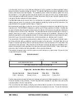
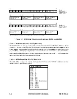
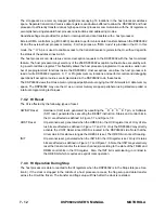
If the current bus cycle is in an enabled memory space, the
—
T
–
T pin is controlled by comparison of the
current bus cycle and the previously latched bus cycle and the current bus cycle information (A, S) is latched
at the end of the bus cycle. Thus the current bus cycle information becomes the previously latched bus cycle
information for comparison in the next enabled external bus cycle. The encoding of the memory space en-
ables is shown in Figure 7-5.
The page circuit normally monitors addresses intended for one external physical memory. However, if mul-
tiple memory spaces are mapped into one physical memory at either the same or different addresses, then
the page circuit must monitor multiple memory spaces. These memory space enable bits allow the user to
indicate which memory spaces should be monitored. Also if multiple memory spaces are mapped into dif-
ferent physical memories which are not accessed in an "interleaved" manner, one page circuit can serve
multiple external physical memories by being enabled for more than one memory space. Non-interleaved
accesses with multiple external physical memories are typical of systems where the main external bus ac-
tivity is block-oriented DMA transfers.
If all three memory space enable bits are cleared, the page circuit is in the Personal Reset state. While in
the Personal Reset state, the page circuit is inactive,
—
T
–
T remains deasserted for all external bus cycles,
and no bus cycle information is latched. The first bus cycle after re-enabling the page circuit always has
—
T
–
T deasserted since no previous bus cycle information is available for comparison.
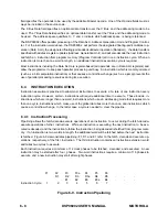
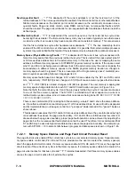
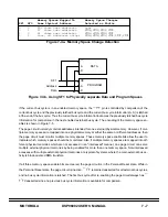
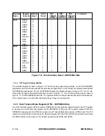
Memory Spaces Mapped To Memory Space Changes
SF1 SF0 Same Physical Address Detected as Faults
0 0 PXY share same addresses none
0 1 PY share same addresses P
→
X,X
→
P,X
→
Y,Y
→
X
1 0 XY share same addresses P
→
X,X
→
P,P
→
Y,Y
→
P
1 1 none, all addresses unique P
→
X,X
→
P,X
→
Y,Y
→
X,P
→
Y,Y
→
P
Figure 7-4a. Memory Space Change Detection
—
PROGRAM
DATA
D
D
A
A
CE
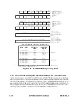
Figure 7-4b. Using SF1 to Physically separate Data and Program Spaces
Data
Address
SF1
Summary of Contents for DSP96002
Page 3: ...1 2 DSP96002 USER S MANUAL MOTOROLA ...
Page 38: ...MOTOROLA DSP96002 USER S MANUAL 3 15 Figure 3 4 Modulo Arithmetic Unit Block Diagram ...
Page 39: ...3 16 DSP96002 USER S MANUAL MOTOROLA ...
Page 53: ...4 14 DSP96002 USER S MANUAL MOTOROLA ...
Page 76: ...MOTOROLA DSP96002 USER S MANUAL 5 23 Figure 5 8 Address Modifier Summary ...
Page 86: ...6 10 DSP96002 USER S MANUAL MOTOROLA ...
Page 101: ...MOTOROLA DSP96002 USER S MANUAL 7 15 Figure 7 9 HI Block Diagram One Port ...
Page 140: ...7 54 DSP96002 USER S MANUAL MOTOROLA ...
Page 166: ...9 10 DSP96002 USER S MANUAL MOTOROLA ...
Page 181: ...MOTOROLA DSP96002 USER S MANUAL 10 15 Figure 10 8 Program Address Bus FIFO ...
Page 337: ...MOTOROLA DSP96002 USER S MANUAL A 149 ...
Page 404: ...A 216 DSP96002 USER S MANUAL MOTOROLA PC xxxx D ...
Page 460: ...A 272 DSP96002 USER S MANUAL MOTOROLA SIOP Not affected ...
Page 484: ...A 296 DSP96002 USER S MANUAL MOTOROLA SSH PC SSL SR SP 1 SP ...
Page 519: ...MOTOROLA DSP96002 USER S MANUAL A 331 ...
Page 718: ...MOTOROLA DSP96002 USER S MANUAL B 199 ...
Page 871: ... MOTOROLA INC 1994 MOTOROLA TECHNICAL DATA SEMICONDUCTOR M Addendum ...
Page 888: ...MOTOROLA INDEX 1 INDEX ...
Page 889: ......

