


A - 4
DSP56000/DSP56001 USER’S MANUAL
MOTOROLA
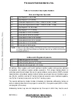
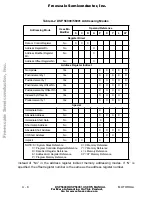
Table A-3 shows the various categories to which each addressing mode belongs. The
following classifications will be used in the instruction descriptions.
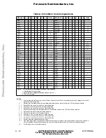
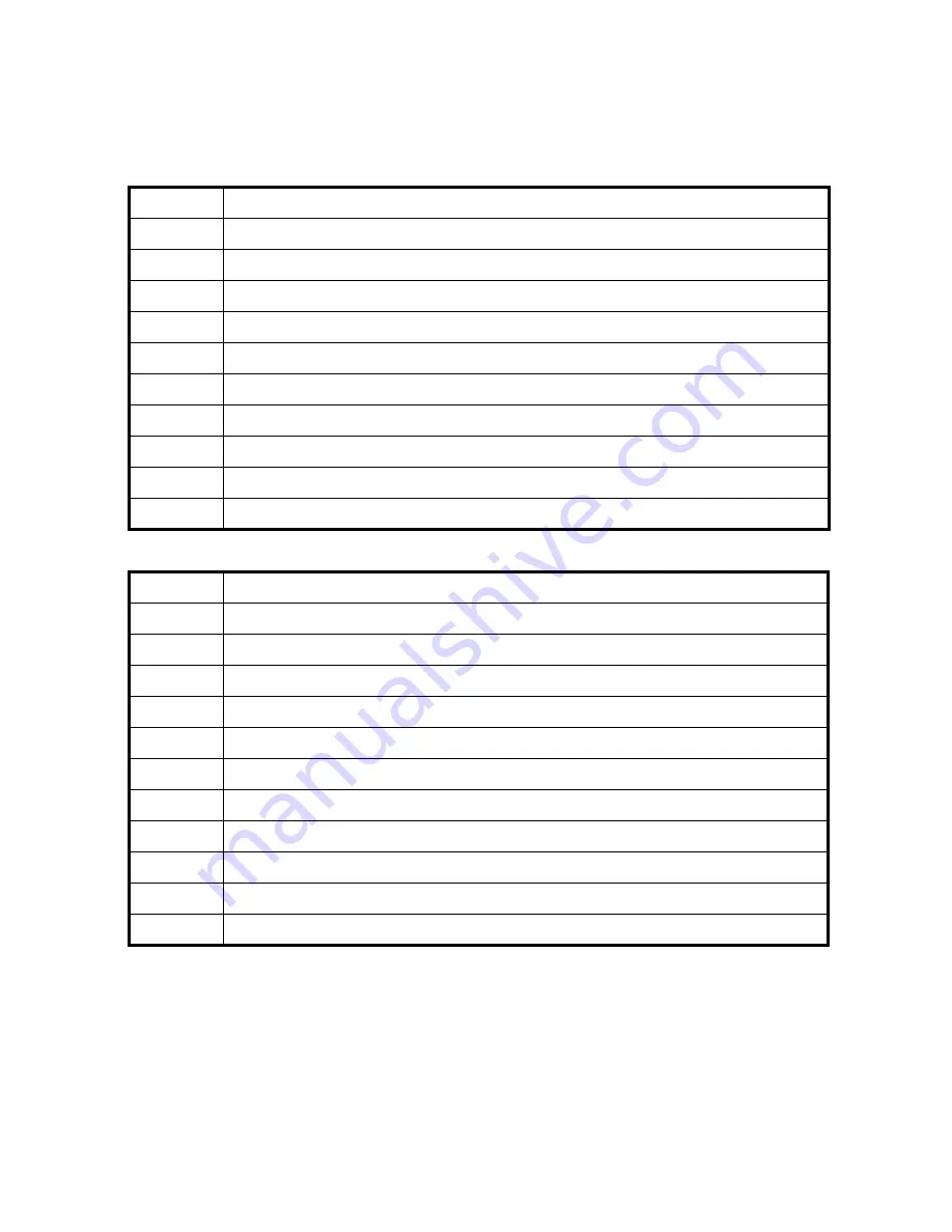
Table A-3. DSP56000/DSP56001 Addressing Mode Encoding
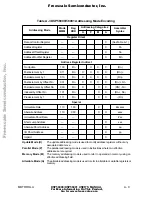
These addressing mode categories may be combined so that additional, more restrictive
classifications may be defined. For example, the instruction descriptions may use a
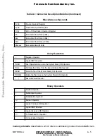
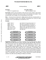
ea
Effective Address
eax
Effective Address for X Bus
eay
Effective Address for Y Bus
xxxx
Absolute Address (16 Bits)
xxx
Short Jump Address (12 Bits)
aa
Absolute Short Address (6 Bits, Zero Extended)
pp
I/O Short Address (6 Bits, Ones Extended)
<. . .>
Specifiies the Contents of the Specified Address
X:
X Memory Reference
Y:
Y Memory Reference
L:
Long Memory Reference = X:Y
P:
Program Memory Reference
Address Operands
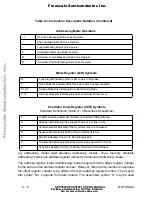
PC
Program Counter Register (16 Bits)
MR
Mode Register (8 Bits)
CCR
Condition Code Register (8 Bits)
SR
Status Register = MR:CCR (16 Bits)
OMR
Operating Mode Register (8 Bits)
LA
Hardware Loop Address Register (16 Bits)
LC
Hardware Loop Counter Register (16 Bits)
SP
System Stack Pointer Register (6 Bits)
SSH
Upper Portion of the Current Top of the Stack (16 Bits)
SSL
Lower Portion of the Current Top of the Stack (16 Bits)
SS
System Stack RAM = SSH: SSL (15 Locations by 32 Bits)
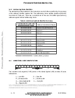
Program Controller Registers Operands
Table A-1 Instruction Description Notation (Continued)
F
re
e
sc
a
le
S
e
m
ic
o
n
d
u
c
to
r,
I
Freescale Semiconductor, Inc.
For More Information On This Product,
Go to: www.freescale.com
n
c
.
..