background image

Chapter 1

MODEL CHART AND TECHNICAL SPECIFICATIONS

1.0

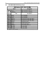
GM140/GM160 Model Chart

GM Series VHF 136-174 MHz

Model

Description

MDM25KKC9AA1_E

GM140, 136-174 MHz, 25-45W, 4 Ch

MDM25KKF9AA5_E

GM160, 136-174 MHz, 25-45W, 128 Ch

Item

Description

X

GCN6112_

Control Head, GM140

X

GCN6114_

Control Head, GM160

X

IMUD6015_S

Field Replaceable Unit (Main Board) GM140

X

IMUD6015_S

Field Replaceable Unit (Main Board) GM160

X

X

ENBN4056_

Packaging, Waris Mobile Radio

X

X

GLN7324_

Low Profile Mounting Trunnion

X

X

HKN9402_

12V Power Cable, 25-45W

X

X

MDRMN4025_

Enhanced Compact Microphone

X

6864110B86

User Guide, GM140

X

6864110B87

User Guide, GM160

X = Indicates one of each is required

Summary of Contents for GM Series

Page 1: ...Professional Radio GM Series VHF 136 174MHz Service Information Issue September 2000 ...

Page 2: ...he copyrighted computer program Accordingly any copyrighted Motorola computer programs contained in the Motorola products described in this manual may not be copied or reproduced in any manner without the express written permission of Motorola Furthermore the purchase of Motorola products shall not be deemed to grant either directly or by implication estoppel or otherwise any license under the cop...

Page 3: ...2 3 0 VHF 136 174MHz Transmitter Power Amplifier PA 25 W 2 3 3 1 First Power Controlled Stage 2 3 3 2 Power Controlled Driver Stage 2 4 3 3 Final Stage 2 4 3 4 Directional Coupler 2 4 3 5 Antenna Switch 2 5 3 6 Harmonic Filter 2 5 3 7 Power Control 2 5 4 0 VHF 136 174MHz Frequency Synthesis 2 6 4 1 Reference Oscillator 2 6 4 2 Fractional N Synthesizer 2 6 4 3 Voltage Controlled Oscillator VCO 2 7 ...

Page 4: ...oubleshooting Flow Chart for 45W Transmitter Sheet 2 of 2 3 4 4 0 Troubleshooting Flow Chart for Synthesizer 3 5 5 0 Troubleshooting Flow Chart for VCO 3 6 Chapter 4 VHF PCB SCHEMATICS PARTS LISTS 1 0 Allocation of Schematics and Circuit Boards 4 1 1 1 Controller Circuits 4 1 2 0 VHF 1 25W PCB 8486172B04 Schematics 4 3 2 1 VHF 1 25W PCB 8486172B04 Parts List 4 10 3 0 VHF 1 25W PCB 8486172B06 Schem...

Page 5: ...ion X GCN6112_ Control Head GM140 X GCN6114_ Control Head GM160 X IMUD6015_S Field Replaceable Unit Main Board GM140 X IMUD6015_S Field Replaceable Unit Main Board GM160 X X ENBN4056_ Packaging Waris Mobile Radio X X GLN7324_ Low Profile Mounting Trunnion X X HKN9402_ 12V Power Cable 25 45W X X MDRMN4025_ Enhanced Compact Microphone X 6864110B86 User Guide GM140 X 6864110B87 User Guide GM160 X Ind...

Page 6: ... GCN6120_ Control Head GM360 X GCN6121_ Control Head GM380 X IMUD6013_S Field Replaceable Unit Main Board GM340 X IMUD6013_S Field Replaceable Unit Main Board GM360 X IMUD6024_S Field Replaceable Unit Main Board GM380 X X X ENBN4056_ Packaging Waris Mobile X X X GLN7324_ Low Profile Mounting Trunnion X X X HKN4137_ 12V Power Cable 1 25W X X X MDRMN4025_ Enhanced Compact Microphone X 6864110B80 Use...

Page 7: ...Control Head GM660 X GCN6121_ Control Head GM1280 X IMUD6018_S Field Replaceable Unit Main Board GM640 X IMUD6018_S Field Replaceable Unit Main Board GM660 X IMUD6018_S Field Replaceable Unit Main Board GM1280 X X X ENBN4056_ Packaging Waris Mobile Radio X X X GLN7324_ Low Profile Mounting Trunnion X X X HKN4137_ 12V Power Cable 1 25W X X X MDRMN4025_ Enhanced Compact Microphone X 6864110B83_ User...

Page 8: ... Dimensions H x W x D mm Depth excluding knobs GM160 360 660 59mm x 179mm x 186mm 1 25W 59mm x 179mm x 198mm 25 45W add 9mm for Volume Knob Dimensions H x W x D mm Depth excluding knobs GM380 1280 188mm x 185mm x 72mm add 8mm for Volume Knob Weight GM140 340 640 1400gr Weight GM160 360 660 1400gr Weight GM380 1280 1500gr Sealing Withstands rain testing per MIL STD 810 C D E and IP54 Shock and Vibr...

Page 9: ... kHz Audio Response 300 3000Hz 1 to 3 dB Audio Distortion 1000Hz 60 Rated Maximum Deviation 3 typical Receiver VHF Frequencies Full Bandsplit VHF 136 174 MHz Channel Spacing 12 5 20 25 kHz Sensitivity 12 dB SINAD 0 30 µV 0 22 µV typical Intermodulation ETS 65 dB Base Mode 70dB 1 25W model only Adjacent Channel Selectivity ETS 65 dB 12 5 kHz 75 dB 20 kHz 80 dB 25 kHz Spurious Rejection ETS 75 dB 12...

Page 10: ...1 6 MODEL CHART AND TECHNICAL SPECIFICATIONS ...

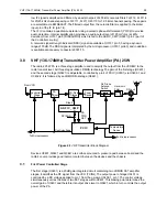
Page 11: ...mixer high IF low IF and receiver back end Two varactor tuned bandpass filters perform antenna signal pre selection A cross over quad diode mixer converts the signal to the first IF of 44 85 MHz High side first injection is used Figure 2 1 VHF Receiver Block Diagram Demodulator 1 Crystal Filter Mixer Varactor Tuned Filter RF Amp Varactor Tuned Filter Antenna Control Voltage from PCIC First LO from...

Page 12: ...f both transistors Q3002 and Q3001 This protects the RF pre amplifier from excessive dissipation during transmit mode A switchable 3dB pad R3022 R3024 R3016 and R3018 controlled via Line FECNTL_2 and Q3021 stabilizes the output impedance and intermodulation performance A second 2 pole varactor tuned bandpass filter provides additional filtering of the amplified signal The dual varactor diode D3004...

Page 13: ...he output from the VCOBIC to the radio transmit level All three stages utilize LDMOS technology The gain of the first stage U3401 and the second stage Q3421 is adjustable controlled by pin 4 of PCIC U3501 via U3402 1 and U3402 2 It is followed by an LDMOS final stage Q3441 Figure 2 1 VHF Transmitter Block Diagram Devices U3401 Q3421 and Q3441 are surface mounted A pressure pad between board and th...

Page 14: ... provides a DC output voltage at pin 4 INT which sets the reference voltage of the current control loop A raising power output causes the DC voltage from the PCIC to fall and U3402 2 adjusts the bias voltage for a lower drain current to lower the gain of the stage In receive mode the DC voltage from PCIC pin 23 RX turns on Q3422 which in turn switches off the biasing voltage to Q3421 3 3 Final Sta...

Page 15: ...portion of the forward RF power from the transmitter is sampled by the directional coupler and rectified to provide a DC voltage to the RFIN port of the PCIC pin 1 which is proportional to the sampled RF power The ASFIC U0221 has internal digital to analog converters DACs which provide a reference voltage of the control loop to the PCIC via R3505 The reference voltage level is programmable through...

Page 16: ... used Y3261 D3261 C3261 C3262 and R3262 are not used and C3263 is increased to 0 1 uF 4 2 Fractional N Synthesizer The LVFRAC N synthesizer IC U3201 consists of a pre scaler a programmable loop divider control divider logic a phase detector a charge pump an A D converter for low frequency digital modulation a balance attenuator to balance the high frequency analog modulation and low frequency digi...

Page 17: ...ates a stable loop IC U3201 provides the 16 8 MHz reference frequency at pin 19 The serial interface SRL is connected to the microprocessor via the data line DATA U3201 7 clock line CLK U3201 8 and chip enable line CSX U3201 9 4 3 Voltage Controlled Oscillator VCO The Voltage Controlled Oscillator VCO consists of the VCO Buffer IC VCOBIC U3301 the TX and RX tank circuits the external RX buffer sta...

Page 18: ...r is controlled by the loop divider which in turn receives its inputs via the SRL The output of the pre scaler is applied to the loop divider The output of the loop divider is connected to the phase detector which compares the loop divider s output signal with the reference signal The reference signal is generated by dividing down the signal of the reference oscillator Y3261 or Y3263 The output si...

Page 19: ...nsmitter Block Diagram Devices U3401 and Q3421 are surface mounted The remaining devices are directly attached to the heat sink 5 1 Power Controlled Stage The first stage U3401 is a 20dB gain integrated circuit containing two LDMOS FET amplifier stages It amplifies the RF signal from the VCO TXINJ The output power of stage U3401 is controlled by a DC voltage applied to pin 1 from the power control...

Page 20: ...e radio s DC supply voltage input PASUPVLTG via L3431 and L3432 5 4 Final Stage The final stage uses the bipolar device Q3441 The device s collector current is also drawn from the radio s DC supply voltage input To maintain class C operation the base is DC grounded by a series inductor L3441 and a bead L3442 A matching network consisting of C3446 52 C3467 L3444 5 and two striplines transforms the ...

Page 21: ...sampled by the directional coupler rectified and summed to provide a DC voltage to the RFIN port of the PCIC pin 1 which is proportional to the sampled RF power The ASFIC contains a digital to analog converter DAC which provides a reference voltage of the control loop to the PCIC via R3517 The reference voltage level is programmable through the SPI line of the PCIC This reference voltage is propor...

Page 22: ...2 12 THEORY OF OPERATION ...

Page 23: ...n the case of no audio OR ELSE go to B Yes No Spray or inject 44 85MHz into XTAL Filter FL3101 Audio heard B Yes No Check 2nd LO 44 395MHz at C3135 LO present B Yes Check voltages on U3101 Biasing OK No No A Yes Check Q3102 bias for faults Replace Q3102 Go to B Yes No Check circuitry around U3101 Replace U3101 if defect Check circuitry around Y3101 Re place Y3101 if defect Voltages OK ...

Page 24: ...9 Inject RF into J3401 Is tuning voltage OK No Yes Check RF amp Q3001 Stage Check filter between C3012 T3001 Yes Check T3001 T3002 D3031 R3030 R3034 L3032 C3034 and C3035 Yes 1st LO level OK Locked Yes Check FGU Yes Trace IF signal from C3035 to Q3101 Check for bad XTAL filter No Yes IF signal at Q3102 collector Before replacing U3101 check U3101 voltages Yes Check for 5VDC Is 9V3 present Check Su...

Page 25: ...3403 to Ground NO YES Voltage at TP3402 rises Check PA Stages NO YES PCIC U3501 Pin 14 9 3V DC Check 9 3V Regulator U0641 NO YES PCIC U3501 Pin 16 4V DC Replace PCIC U3501 NO YES TP3404 9 1V DC If U3201 Pin 2 is high replace PCIC U3501 otherwise check controller and FGU YES NO TP3403 0 5V DC Replace PCIC U3501 Check Forward Power Sense Circuit D3451 Check Forward Power Sense Circuit D3451 NO YES P...

Page 26: ...n 3 8 8V Check S3440 R3442 and R3443 YES Pin 3Voltage 0 51 Voltage at Pin 1 NO Replace U3401 2V DCVoltage at U3402 2 Pin 7 6V Check Components between U3402 2 Pin7 and Q3421 Check Resistive Network at Pins 5 6 before repla cing Q3421 YES DCVoltage at U3402 2 Pin 5 8 8V Check Components bet ween U3402 2 Pin7 and Q3421 Check Resistive Network at Pins 5 6 before replacing Q3421 NO Check Q3422 NO Chec...

Page 27: ...e U3401 Pin 6 3V Supply Replace Q3441 Check FGU U3301 NO Check Components between TP3401 C3417 NO YES ASFIC U0221 Pin 6 1 4V DC Check Bias Tuning before replacing ASFIC U0221 Check Components between ASFIC and Q3441 before repla cing Q3441 YES RF Voltage Q3421 Gate 1V NO Check Components between C3417 Q3421 YES RF Voltage Q3441 Gate 4V NO Check Components between Q3421 Q3441 Check Components betwe...

Page 28: ...U3501 Pin 4 Short TP3403 to Ground NO YES Voltage at TP3402 ris es Check PA Stages NO YES PCIC U3501 Pin 15 9 3V DC Check 9 3 V Regulator U0641 NO YES PCIC U3501 Pin 16 4V DC Replace PCIC U3501 NO YES TP3404 9 1V DC If U3201 Pin 3 is high replace PCIC U3501 otherwise check controller and FGU YES NO TP3403 0 5V DC Replace PCIC U3501 Check Forward Reverse Power Sense Circuitry D3451 D3452 Check Forw...

Page 29: ...ace U3401 Replace Q3421 NO 0V 1 4V Bias 2 DC Voltage at TP3407 YES RF Voltage at TP3401 100mV YES RF Voltage U3401 Pin 6 3V Replace Q3421 Supply Replace Q3431 Check FGU U3301 NO Check Components between TP3401 C3417 NO YES ASFIC U0221 Pin 6 1 4V DC Check Bias Tuning be fore replacing ASFIC U0221 Check Components between ASFIC and Q3431 before re placing Q3431 YES RF Voltage Q3421 Gate 1V NO Check ...

Page 30: ...ts Is there a short between Pin 47 and Pins 14 15 of U3201 Replace or resolder necessary components Is RF level at U3201 Pin 32 12 x 25 dBm Are R3221 R3222 R3223 C3221 C3222 C3224 OK Replace U3201 If R3227 C3226 C3227 are OK then see VCO troubleshooting chart Are Waveforms at Pins 14 15 triangular Do Pins 7 8 9 of U3201 toggle when channel is changed Check programming lines between U0101 and U3201...

Page 31: ...eplace R3364 NO NO YES YES If R3402 and C3315 are OK replace U3301 TX VCO RX VCO Correct Problem Visual check of board OK Make sure U3211 is working correctly and runner between U3211 Pin 1 and U3301 Pin 14 18 is OK Check runner between U3201 Pin 2 and U3301 Pin 19 Is RF available If all parts from U3301 Pin 8 to Base of Q3301 are OK replace U3301 If all parts associated with the pins are OK repla...

Page 32: ...3 10 TROUBLESHOOTING CHARTS ...

Page 33: ... schematics and the related PCB and parts list are shown in the tables below Table 4 1 VHF 1 25W Diagrams and Parts Lists PCB 8486172B04 Main Board Top Side 8486172B04 Main Board Bottom Side Page 4 3 Page 4 4 SCHEMATICS Power Amplifier 1 25W FRACN Voltage Controlled Oscillator Receiver Front End IF Page 4 5 Page 4 6 Page 4 7 Page 4 8 Page 4 9 Parts List 8486172B04 Page 4 10 Table 4 2 VHF 1 25W Dia...

Page 34: ...illator Receiver Front End IF FRACN Page 4 15 Page 4 17 Page 4 18 Page 4 25 Page 4 26 Parts List 8486172B07 Page 4 27 Table 4 4 VHF 25 45W Diagrams and Parts Lists PCB 8486140B12 Main Board Top Side 8486140B12 Main Board Bottom Side Page 4 30 Page 4 31 SCHEMATICS Power Amplifier 25 45W FRACN Voltage Controlled Oscillator Receiver Front End IF Page 4 32 Page 4 26 Page 4 17 Page 4 18 Page 4 25 Parts...

Reviews: