Theory of Operation
7-7
The serial interface (SPI_DATA) is connected to the microprocessor via the data
line (pin 5 of U5702), clock line (pin 6 of U5702), and chip enable line (pin 5 of
U5702). Proper enabling of these lines should allow the microprocessor to load
the synthesizer IC.
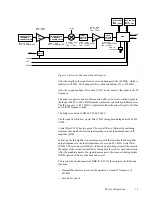
The output of the VCO is fed into the buffer input port (pin 1) of U5701. The
output of the buffer, pin 5 of U5701, is applied to the input of the feedback
amplifier (Q5703) through an attenuator network (R5735, R5733, R5732). To
close the synthesizer loop, the output of Q5703 is connected to the PREIN port
(pin 20) of synthesizer U5702. The buffer output (pin 5 of U5701) also provides
signal for the receiver LO injection and transmit injection string circuit. The
charge pump current is present at pin 31 of U5702.
The loop filter (which consists of R5716, R5717, R5734, C5750, C5744, C5745,
C5736, C5746, C5747, C5794, C5795, C5796, C5797, C5798, C5799) will then
transform this current into a voltage that will, in turn, be applied to Vcontrol of the
VCOs and alter the output frequency.
In order to modulate the PLL, the two-point modulation method is utilized. The
audio signal is applied to both the A/D converter (low frequency path) as well as
the balance attenuator (high frequency path) via pin 8 on U5702.
The A/D converter will convert the low-frequency, analog modulating signal into
a digital code that will in turn be applied to the loop divider. This will cause the
carrier to deviate. The balance attenuator is used to adjust the VCO deviation
sensitivity to high frequency modulating signals. The output of the balance
attenuator is present at the MODOUT port (pin 28 of U5702).
The transmit injection string consists of two amplifier stages (Q5707 & Q5705)
whose main purpose is to maintain a constant output to drive the RFPA and
provide isolation. The Q5705 stage is actively biased through Q5701, and Q5707
has passive bias. The TX injection string is on, only during the transmit mode (K
9.1V line is at 9.1 V).
There are two VCOs, one for the 806-825 band that is used as LO INJ. during
receive and TX INJ. at conventional mode. The second VCO is used as TX INJ.
in the talk-around mode.
The VCOs get their control voltage through L5702 and L5701. Q5704 and Q5706
are the oscillation transistors. C5793, C5792 and C5785, C5784 are the oscillator
feedback capacitors. U5707 and U5706 are micro strip resonators. CR5702 and
CR5701 are the varactors. C5790 and C5782 determine the KV. C5703 and C5704
determine the VCO operation frequency.
C5791 and C5783 are the coupling capacitors between the tank and the oscillation
transistor.
The two VCOs are coupled to the buffer (Q5702) through C5789 and C5786. The
stage output signal is fed to U5701 input (pin 1) through C5770 & R5736.

