MEVB SUPPORT INFORMATION
M68MPB916X1UM/D
4-3
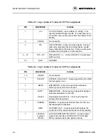
Table 4-3. Logic Analyzer Connector J9 Pin Assignments
PIN
MNEMONIC
SIGNAL
1, 2
SPARE
No connection
3
OE(H)
I/O PRU OUTPUT ENABLE – Input, active high; when
low disables the port H outputs.
4 – 11
PH7 – PH0
PORT H I/O SIGNALS – PRU replacement of the port
H function.
12 – 19
PG7 – PG0
PORT G I/O SIGNALS – PRU replacement of the port
G function.
20
GND
GROUND
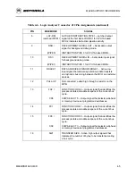
Table 4-4. Logic Analyzer Connector J10 Pin Assignments
PIN
MNEMONIC
SIGNAL
1
+5V
+5 VDC POWER – Input voltage (+5 Vdc @ 1.0 A)
used by the MEVB logic circuits. (To make this pin no
connection, remove the jumper from the header on the
MPFB.)
2
SPARE
No connection
3
AS
ADDRESS STROBE – Active-low output signal that
indicates whether a valid address is on the address
bus.
4 – 19
A15 – A0
ADDRESS BUS BITS 15 – 0 – Sixteen bits of the 24-bit
address bus.
20
GND
GROUND


