MEVB SUPPORT INFORMATION
4-6
M68MPB916X1UM/D
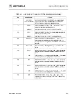
Table 4-6. Logic Analyzer Connector J12 Pin Assignments (continued)
PIN
MNEMONIC
SIGNAL
17
SIZ0
TRANSFER SIZE – Active-high output signals that
indicates the number of bytes to be transferred during a
bus cycle.
18
R/W
READ/WRITE – Active-high output signal that indicates
the direction of data transfer on the bus.
19
BGACK /
CSE
BUS GRANT ACKNOWLEDGE – Active-low input
signal that indicates an external device has assumed
bus mastership.
EMULATOR CHIP SELECT – Active-low output signal
that selects external emulation devices at internally-
mapped addresses. CSE is used to emulate I/O ports.
20
GND
GROUND
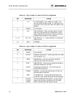
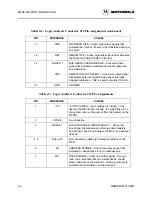
Table 4-7. Logic Analyzer Connector J13 Pin Assignments
PIN
MNEMONIC
SIGNAL
1
+5V
+5 VDC POWER – Input voltage (+5 Vdc @ 1.0 A)
used by the MEVB logic circuits. (To make this pin no
connection, remove the jumper from the header on the
MPFB.)
2
SPARE
No connection
3
DSACK1
DATA AND SIZE ACKNOWLEDGE 1 – Active-low
input signal that allows asynchronous data transfers
and dynamic bus sizing between the MCU and external
devices.
4, 5
PULL-UP
Not connected; pulled high through a resistor on the
MPB.
6
AS
ADDRESS STROBE – Active-low output signal that
indicates a valid address is on the address bus.
7
DS
DATA STROBE – Active-low output signal. During a
read cycle, indicates that an external device should
place valid data on the data bus. During a write cycle,
indicates that valid data is on the data bus.


