68000 Motherboard User’s Manual
Rev. A
Page 18 of 54
6.2
Glimpse of the 68000
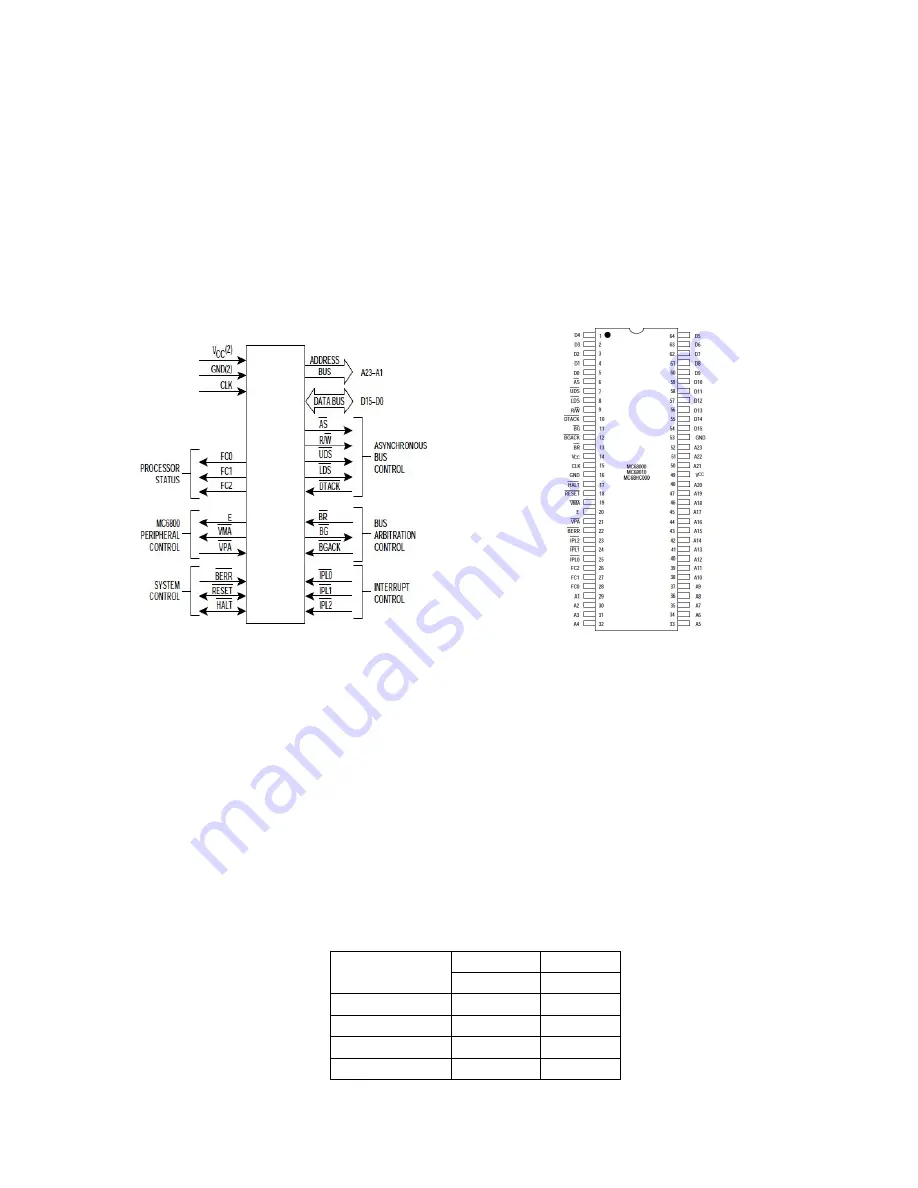
With greater detail coming into focus, refer to Figure 6 showing the signals of the 68000
microprocessor. The pin diagram of the DIP chip is also given in Figure 7 for reference.
The Data and Address buses are shown, as well as the various control signaling. The
functions and interactions of these signals are discussed in subsequent sections. For
deeper detail, refer to the Motorola M68000 8-/16-/32-bit Microprocessors User’s
Manual.
Figure 6: 68000 Input and Output
Signals
Figure 7: 68000 DIP Pin Diagram
6.3
Bus Architecture of the 68000
The 16-bit 68000 data bus is comprised of two conjoined 8-bit data buses. They are
referred to as the upper and lower data buses, or informally the ‘hi’ and ‘lo.’ The upper
bus carries the most significant byte data (D8-15), and the lower carries the least
significant byte (D0-D7). Since the 68000 uses a big-endian byte ordering convention,
lower addresses are associated with bytes of higher significance. That is, the high bytes
reside in the ‘hi’ device, and occupy the lower memory address. The low bytes reside in
the ‘lo’ device, and occur in the higher memory address.
Table 7: 68000 Byte Ordering Convention, Big-Endian
+0
+1
Address
Even
Odd
Significance
MSB
LSB
Data Lines
D15-D8
D7-D0
Control Line
/UDS
/LDS
Device
‘Hi’
‘Lo’
Summary of Contents for MB68k-100
Page 1: ...Rev A Grant K c 2011 ...


