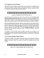
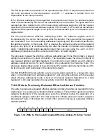
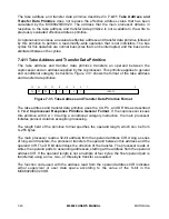
background image

MOTOROLA

M68020 USER’S MANUAL

7- 47

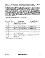
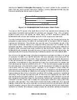
described in Section 6 Exception Processing. The vector number for the exception is
taken from the vector number field of the primitive, and the MC68020/EC020 uses the
four-word stack frame format shown in Figure 7-41.

0

11

12

15

STATUS REGISTER

0

0

0

0

VECTOR NUMBER

PROGRAM COUNTER

+06

+02

SP

Figure 7-41. MC68020/EC020 Preinstruction Stack Frame

The value of the PC saved in this stack frame is the F-line operation word address of the
coprocessor instruction during which the primitive was received. Thus, if the exception
handler routine does not modify the stack frame, an RTE instruction causes the
MC68020/EC020 to return and reinitiate execution of the coprocessor instruction.

The take preinstruction exception primitive can be used when the coprocessor does not
recognize a value written to either its command CIR or condition CIR to initiate a
coprocessor instruction. This primitive can also be used if an exception occurs in the
coprocessor instruction before any program-visible resources are modified by the
instruction operation. This primitive should not be used during a coprocessor instruction if
program-visible resources have been modified by that instruction. Otherwise, since the
MC68020/EC020 reinitiates the instruction when it returns from exception processing, the
restarted instruction receives the previously modified resources in an inconsistent state.

One of the most important uses of the take preinstruction exception primitive is to signal
an exception condition in a cpGEN instruction that was executing concurrently with the
main processor's instruction execution. If the coprocessor no longer requires the services
of the main processor to complete a cpGEN instruction and if the concurrent instruction
completion is transparent to the programming model, the coprocessor can release the
main processor by issuing a primitive with CA = 0. The main processor usually executes
the next instruction in the instruction stream, and the coprocessor completes its operations
concurrently with the main processor operation. If an exception occurs while the
coprocessor is executing an instruction concurrently, the exception is not processed until
the main processor attempts to initiate the next general or conditional instruction. After the
main processor writes to the command or condition CIR to initiate a general or conditional
instruction, it then reads the response CIR. At this time, the coprocessor can return the
take preinstruction exception primitive. This protocol allows the main processor to proceed
with exception processing related to the previous concurrently executing coprocessor
instruction and then return and reinitiate the coprocessor instruction during which the
exception was signaled. The coprocessor should record the addresses of all general
category instructions that can be executed concurrently with the main processor and that
support exception recovery. Since the exception is not reported until the next coprocessor
instruction is initiated, the processor usually requires the instruction address to determine

Summary of Contents for MC68020

Page 1: ...sustain life or for any other application in which the failure of the Motorola product could create a situation where personal injury or death may occur Should Buyer purchase or use Motorola products for any such unintended or unauthorized application Buyer shall indemnify and hold Motorola and its officers employees subsidiaries affiliates and distributors harmless against all claims costs damage...

Page 2: ...of the following sections Section 1 Introduction Section 2 Processing States Section 3 Signal Description Section 4 On Chip Cache Memory Section 5 Bus Operation Section 6 Exception Processing Section 7 Coprocessor Interface Description Section 8 Instruction Execution Timing Section 9 Applications Information Section 10 Electrical Characteristics Section 11 Ordering Information and Mechanical Data ...

Page 3: ...tes 2 1 Privilege Levels 2 2 2 1 1 Supervisor Privilege Level 2 2 2 1 2 User Privilege Level 2 3 2 1 3 Changing Privilege Level 2 3 2 2 Address Space Types 2 4 2 3 Exception Processing 2 5 2 3 1 Exception Vectors 2 5 2 3 2 Exception Stack Frame 2 6 Section 3 Signal Description 3 1 Signal Index 3 2 3 2 Function Code Signals FC2 FC0 3 2 3 3 Address Bus A31 A0 MC68020 A23 A0 MC68EC020 3 2 3 4 Data Bu...

Page 4: ...rmination Signals 5 4 5 2 Data Transfer Mechanism 5 5 5 2 1 Dynamic Bus Sizing 5 5 5 2 2 Misaligned Operands 5 14 5 2 3 Effects of Dynamic Bus Sizing and Operand Misalignment 5 20 5 2 4 Address Size and Data Bus Relationships 5 21 5 2 5 Cache Interactions 5 22 5 2 6 Bus Operation 5 24 5 2 7 Synchronous Operation with DSACK1 DSACK0 5 24 5 3 Data Transfer Cycles 5 25 5 3 1 Read Cycle 5 26 5 3 2 Writ...

Page 5: ...ol MC68EC020 5 73 5 8 Reset Operation 5 76 Section 6 Exception Processing 6 1 Exception Processing Sequence 6 1 6 1 1 Reset Exception 6 4 6 1 2 Bus Error Exception 6 4 6 1 3 Address Error Exception 6 6 6 1 4 Instruction Trap Exception 6 6 6 1 5 Illegal Instruction and Unimplemented Instruction Exceptions 6 7 6 1 6 Privilege Violation Exception 6 8 6 1 7 Trace Exception 6 9 6 1 8 Format Error Excep...

Page 6: ...on 7 12 7 2 2 1 1 Format 7 12 7 2 2 1 2 Protocol 7 12 7 2 2 2 Set on Coprocessor Condition Instruction 7 13 7 2 2 2 1 Format 7 13 7 2 2 2 2 Protocol 7 14 7 2 2 3 Test Coprocessor Condition Decrement and Branch Instruction 7 14 7 2 2 3 1 Format 7 14 7 2 2 3 2 Protocol 7 15 7 2 2 4 Trap on Coprocessor Condition Instruction 7 15 7 2 2 4 1 Format 7 15 7 2 2 4 2 Protocol 7 16 7 2 3 Coprocessor Context ...

Page 7: ...o Previously Evaluated Effective Address Primitive 7 37 7 4 11 Take Address and Transfer Data Primitive 7 39 7 4 12 Transfer to from Top of Stack Primitive 7 40 7 4 13 Transfer Single Main Processor Register Primitive 7 40 7 4 14 Transfer Main Processor Control Register Primitive 7 41 7 4 15 Transfer Multiple Main Processor Registers Primitive 7 42 7 4 16 Transfer Multiple Coprocessor Registers Pr...

Page 8: ...1 Fetch Effective Address 8 13 8 2 2 Fetch Immediate Effective Address 8 14 8 2 3 Calculate Effective Address 8 16 8 2 4 Calculate Immediate Effective Address 8 17 8 2 5 Jump Effective Address 8 19 8 2 6 MOVE Instruction 8 20 8 2 7 Special Purpose MOVE Instruction 8 29 8 2 8 Arithmetic Logical Instructions 8 30 8 2 9 Immediate Arithmetic Logical Instructions 8 31 8 2 10 Binary Coded Decimal Operat...

Page 9: ...stics 10 5 Section 11 Ordering Information and Mechanical Data 11 1 Standard Ordering Information 11 1 11 1 1 Standard MC68020 Ordering Information 11 1 11 1 2 Standard MC68EC020 Ordering Information 11 1 11 2 Pin Assignments and Package Dimensions 11 2 11 2 1 MC68020 RC and RP Suffix Pin Assignment 11 2 11 2 2 MC68020 RC Suffix Package Dimensions 11 3 11 2 3 MC68020 RP Suffix Package Dimensions 1...

Page 10: ... 11 5 7 Word Operand Write to Byte Port Example 5 12 5 8 Word Operand Write to Byte Port Timing 5 13 5 9 Misaligned Long Word Operand Write to Word Port Example 5 14 5 10 Misaligned Long Word Operand Write to Word Port Timing 5 15 5 11 Misaligned Long Word Operand Read from Word Port Example 5 16 5 12 Misaligned Word Operand Write to Word Port Example 5 16 5 13 Misaligned Word Operand Write to Wor...

Page 11: ... 42 MC68020 Bus Arbitration Flowchart for Single Request 5 64 5 43 MC68020 Bus Arbitration Operation Timing for Single Request 5 65 5 44 MC68020 Bus Arbitration State Diagram 5 67 5 45 MC68020 Bus Arbitration Operation Timing Bus Inactive 5 69 5 46 MC68EC020 Bus Arbitration Flowchart for Single Request 5 71 5 47 MC68EC020 Bus Arbitration Operation Timing for Single Request 5 72 5 48 MC68EC020 Bus ...

Page 12: ...26 7 21 Operand Alignment for Operand CIR Accesses 7 26 7 22 Coprocessor Response Primitive Format 7 28 7 23 Busy Primitive Format 7 30 7 24 Null Primitive Format 7 31 7 25 Supervisor Check Primitive Format 7 33 7 26 Transfer Operation Word Primitive Format 7 33 7 27 Transfer from Instruction Stream Primitive Format 7 34 7 28 Evaluate and Transfer Effective Address Primitive Format 7 35 7 29 Evalu...

Page 13: ...AL 9 3 9 3 Chip Select PAL Equations 9 4 9 4 Bus Cycle Timing Diagram 9 4 9 5 Example MC68020 EC020 Byte Select PAL System Configuration 9 7 9 6 MC68020 EC020 Byte Select PAL Equations 9 8 9 7 High Resolution Clock Controller 9 11 9 8 Alternate Clock Solution 9 11 9 9 Access Time Computation Diagram 9 12 9 10 Module Descriptor Format 9 15 9 11 Module Entry Word 9 15 9 12 Module Call Stack Frame 9 ...

Page 14: ... Bus Cycles 5 20 5 7 Data Bus Byte Enable Signals for Byte Word and Long Word Ports 5 22 5 8 DSACK1 DSACK0 BERR HALT Assertion Results 5 54 6 1 Exception Vector Assignments 6 3 6 2 Tracing Control 6 9 6 3 Interrupt Levels and Mask Values 6 12 6 4 Exception Priority Groups 6 18 6 5 Exception Stack Frames 6 26 7 1 cpTRAPcc Opmode Encodings 7 16 7 2 Coprocessor Format Word Encodings 7 18 7 3 Null Cop...

Page 15: ... Assignments MC68EC020 PQFP FG Sufffix 9 10 9 4 Memory Access Time Equations at 16 67 and 25 MHz 9 13 9 5 Calculated tAVDV Values for Operation at Frequencies Less Than or Equal to the CPU Maximum Frequency Rating 9 14 9 6 Access Status Register Codes 9 18 10 1 θJA vs Airflow MC68020 CQFP Package 10 3 10 2 Power vs Rated Frequency at TJ Maximum 110 C 10 3 10 3 Temperature Rise of Board vs PD MC680...

Page 16: ...9 29 95 SECTION 1 OVERVIEW UM Rev 1 0 xx M68020 USER S MANUAL MOTOROLA ...

Page 17: ...miconductor IEEE Institute of Electrical and Electronic Engineers ISP Interrupt Stack Pointer LMB Lower Middle Byte LRAR Limited Rate Auto Request LSB Least Significant Byte MMU Memory Management Unit MPU Microprocessor Unit MSB Most Significant Byte MSP Master Stack Pointer NMOS n Type Metal Oxide Semiconductor PAL Programmable Array Logic PC Program Counter PGA Pin Grid Array PMMU Paged Memory M...

Page 18: ...multiplexed bus with 32 bits of address and 32 bits of data The processor supports a dynamic bus sizing mechanism that allows the processor to transfer operands to or from external devices while automatically determining device port size on a cycle by cycle basis The dynamic bus interface allows access to devices of differing data bus widths in addition to eliminating all data alignment restrictio...

Page 19: ...ree of Internal Parallelism Allowing Multiple Instructions To Be Executed Concurrently High Performance Asynchronous Bus Is Nonmultiplexed and Full 32 Bits Dynamic Bus Sizing Efficiently Supports 8 16 32 Bit Memories and Peripherals Full Support of Virtual Memory and Virtual Machine Sixteen 32 Bit General Purpose Data and Address Registers Two 32 Bit Supervisor Stack Pointers and Five Special Purp...

Page 20: ...UCTION PIPE INSTRUCTION ADDRESS BUS ADDRESS SECTION PROGRAM COUNTER SECTION DATA SECTION EXECUTION UNIT MISALIGNMENT MULTIPLEXER SIZE MULTIPLEXER WRITE PENDING BUFFER PREFETCH PENDING BUFFER MICROBUS CONTROL LOGIC BUS CONTROLLER BUS CONTROL SIGNALS ADDRESS BUS ADDRESS PADS DATA PADS DATA BUS 32 BIT ADDRESS BUS 32 BIT 24 Bit for MC68EC020 Figure 1 1 MC68020 EC020 Block Diagram ...

Page 21: ...pervisor programming model contains all the controls to access and enable the special features of the MC68020 EC020 All application software written to run at the nonprivileged user level migrates to the MC68020 EC020 from any M68000 platform without modification Registers D7 D0 are data registers used for bit and bit field 1 to 32 bits byte 8 bit word 16 bit long word 32 bit and quad word 64 bit ...

Page 22: ... 7 8 15 16 31 D0 D1 D2 D3 D4 D5 D6 D7 DATA REGISTERS 0 15 16 31 A0 A1 A2 A3 A4 A5 A6 ADDRESS REGISTERS 0 15 16 31 A7 USP PC CCR CONDITION CODE REGISTER 7 8 0 31 15 0 PROGRAM COUNTER USER STACK POINTER 0 Figure 1 2 User Programming Model ...

Page 23: ...0 31 CACHE ADDRESS REGISTER CACHE CONTROL REGISTER 15 16 15 0 0 0 31 CCR 0 2 3 31 31 SFC A7 ISP A7 MSP INTERRUPT STACK POINTER MASTER STACK POINTER STATUS REGISTER VECTOR BASE REGISTER DFC ALTERNATE FUNCTION CODE REGISTERS Figure 1 3 Supervisor Programming Model Supplement ...

Page 24: ...LEVEL MASTER INTERRUPT MODE CARRY OVERFLOW ZERO NEGATIVE EXTEND Figure 1 4 Status Register SR The VBR contains the base address of the exception vector table in memory The displacement of an exception vector is added to the value in this register to access the vector table The alternate function code registers SFC and DFC contain 3 bit function codes For the MC68020 function codes can be considere...

Page 25: ...emory addresses The coprocessor mechanism allows direct support of floating point operations with the MC68881 and MC68882 floating point coprocessors as well as specialized user defined data types and functions The 18 addressing modes listed in Table 1 1 include nine basic types 1 Register Direct 2 Register Indirect 3 Register Indirect with Index 4 Memory Indirect 5 PC Indirect with Displacement 6...

Page 26: ... L Immediate data NOTE Dn Data Register D7 D0 An Address Register A7 A0 d8 d16 A twos complement or sign extended displacement added as part of the effective address calculation size is 8 d8 or 16 d16 bits when omitted assemblers use a value of zero Xn Address or data register used as an index register form is Xn SIZE SCALE where SIZE is W or L indicates index register size and SCALE is 1 2 4 or 8...

Page 27: ...evices that are not physically present in the system such as tape drives disk drives printers terminals and so forth With proper software emulation a physical system can appear to be any other M68000 computer system to a user program and the program can be given full access to all of the resources of that emulated system Such an emulated system is called a virtual machine 1 5 1 Virtual Memory A sy...

Page 28: ... Subroutine RTE Return from Exception BTST Test Bit RTM Return from Module CALLM Call Module RTR Return and Restore Codes CAS Compare and Swap Operands RTS Return from Subroutine CAS2 Compare and Swap Dual Operands SBCD Subtract Decimal with Extend CHK Check Register Against Bound Scc Set Conditionally CHK2 Check Register Against Upper and Lower Bound STOP Stop CLR Clear SUB Subtract CMP Compare S...

Page 29: ... and the function of the register is emulated by software 1 6 PIPELINED ARCHITECTURE The MC68020 EC020 contains a three word instruction pipe where instruction opcodes are decoded As shown in Figure 1 5 instruction words instruction operation words and all extension words enter the pipe at stage B and proceed to stages C and D An instruction word is completely decoded when it reaches stage D of th...

Page 30: ...etch requests are simultaneously submitted to the cache holding register the instruction cache and the bus controller Thus even if the instruction cache is disabled an instruction prefetch may hit in the cache holding register and cause an external bus cycle to be aborted 1 7 CACHE MEMORY Due to locality of reference instructions that are used in a program have a high probability of being reused w...

Page 31: ...xception handler routine begins The processor enters the exception processing state when an interrupt is acknowledged when an instruction is traced or results in a trap or when some other exception condition arises Execution of certain instructions or unusual conditions occurring during the execution of any instruction can cause exceptions External conditions such as interrupts bus errors and some...

Page 32: ...s and all instructions are executable The bus cycles for instructions executed at the supervisor level are normally classified as supervisor references and the values of the FC2 FC0 signals refer to supervisor address spaces In a multitasking operating system it is more efficient to have a supervisor stack space associated with each user task and a separate stack space for interrupt associated tas...

Page 33: ...uted at the user privilege level are classified as user references and the values of the FC2 FC0 signals specify user address spaces While the processor is at the user level references to the system stack pointer implicitly or to address register seven A7 explicitly refer to the USP 2 1 3 Changing Privilege Level To change from the user to the supervisor privilege level one of the conditions that ...

Page 34: ...rogram Space 0 1 1 Undefined Reserved 1 0 0 Undefined Reserved 1 0 1 Supervisor Data Space 1 1 0 Supervisor Program Space 1 1 1 CPU Space Address space 3 is reserved for user definition 0 and 4 are reserved for future use by Motorola The memory locations of user program and data accesses are not predefined neither are the locations of supervisor data space During reset the first two long words beg...

Page 35: ...or table which consists of 256 exception vectors Exception vectors contain the memory addresses of routines that begin execution at the completion of exception processing These routines perform a series of operations appropriate for the corresponding exceptions Because the exception vectors contain memory addresses each consists of one long word except for the reset vector The reset vector consist...

Page 36: ... format field The frame format field identifies the type of stack frame The RTE instruction uses the value in the format field to properly restore the information stored in the stack frame and to deallocate the stack space The general form of the exception stack frame is illustrated in Figure 2 1 Refer to Section 6 Exception Processing for a complete list of exception stack frames 0 15 SSP 12 FORM...

Page 37: ...re used to specify forcing a signal to a particular state In particular assertion and assert refer to a signal that is active or true negation and negate indicate a signal that is inactive or false These terms are used independently of the voltage level high or low that they represent FC2 FC0 A31 A0 D31 D0 FUNCTION CODES ADDRESS BUS DATA BUS TRANSFER SIZE ASYNCHRONOUS BUS CONTROL EMULATOR SUPPORT ...

Page 38: ...three state outputs provide the address for the current bus cycle except in the CPU address space Refer to Section 2 Processing States for more information on the CPU address space A31 is the most significant address signal for the MC68020 A23 is the most significant address signal for the MC68EC020 The upper eight bits A31 A24 are used internally by the MC68EC020 to access the internal instructio...

Page 39: ...data bus by the MC68020 EC020 Data Buffer Enable DBEN Provides an enable signal for external data buffers Data Transfer and Size Acknowledge DSACK1 DSACK0 Bus response signals that indicate the requested data transfer operation has completed In addition these two lines indicate the size of the external bus port on a cycle by cycle basis and are used for asynchronous transfers Interrupt Priority Le...

Page 40: ...bus cycle A high level indicates a read cycle a low level indicates a write cycle Refer to Section 5 Bus Operation for information about the relationship of R W to bus operation Read Modify Write Cycle RMC This three state output signal identifies the current bus cycle as part of an indivisible read modify write operation it remains asserted during all bus cycles of the read modify write operation...

Page 41: ...signals provide an indication of an interrupt condition and the encoding of the interrupt level from a peripheral or external prioritizing circuitry IPL2 is the most significant bit of the level number For example since the IPL2 IPL0 signals are active low IPL2 IPL0 equal to 5 corresponds to an interrupt request at interrupt level 2 Refer to Section 6 Exception Processing for information on MC6802...

Page 42: ...us Operation and Appendix A Interfacing an MC68EC020 to a DMA Device That Supports a Three Wire Bus Arbitration Protocol for more information on MC68EC020 bus arbitration Bus Grant Acknowledge BGACK MC68020 only This input signal indicates that an external device has become the bus master Refer to Section 5 Bus Operation for more information on MC68020 bus arbitration Refer to Section 5 Bus Operat...

Page 43: ...ore detailed information on emulation support Cache Disable CDIS This input signal statically disables the on chip cache to assist emulator support Refer to Section 4 On Chip Cache Memory for information about the cache refer to Section 9 Applications Information for a description of the use of this signal by an emulator CDIS does not flush the instruction cache entries remain unaltered and become...

Page 44: ...put Low No External Cycle Start ECS Output Low No Read Write R W Output High Low Yes Read Modify Write Cycle RMC Output Low Yes Address Strobe AS Output Low Yes Data Strobe DS Output Low Yes Data Buffer Enable DBEN Output Low Yes Data Transfer and Size Acknowledge DSACK1 DSACK0 Input Low Interrupt Priority Level IPL2 IPL0 Input Low Interrupt Pending IPEND Output Low No Autovector AVEC Input Low Bu...

Page 45: ...lid bit and 32 bits two words of instruction data Figure 4 1 shows a block diagram of the on chip cache organization Externally the MC68EC020 does not use the upper eight bits of the address A31 A24 and addresses FF000000 and 00000000 from the MC68EC020 appear the same However the MC68EC020 does use A31 A24 internally in the instruction cache address tag and addresses FF000000 and 00000000 appear ...

Page 46: ...This index selects one of the 64 entries in the cache Next A31 A8 and FC2 are compared to the tag of the selected entry Note that in the MC68EC020 A31 A24 are used for internal on chip cache tag comparison If there is a match and the valid bit is set a cache hit occurs A1 is then used to select the proper word from the cache entry and the cycle ends If there is no match or if the valid bit is clea...

Page 47: ...eset Four of the bits 3 0 control the instruction cache Bits 31 4 are reserved for Motorola definition They are read as zeros and are ignored when written For future compatibility writes should not set these bits 0 31 E 1 F 2 CE 3 C 4 0 5 0 6 0 7 0 8 0 Figure 4 2 Cache Control Register C Clear Cache The C bit is set to clear all entries in the instruction cache Operating systems and other software...

Page 48: ...y enables the instruction cache but it can clear the E bit for system debugging or emulation as required Disabling the instruction cache does not flush the entries If the cache is reenabled the previously valid entries remain valid and may be used 4 3 2 Cache Address Register CAAR The format of the 32 bit CAAR is shown in Figure 4 3 0 31 RESERVED 1 2 INDEX 7 8 RESERVED Figure 4 3 Cache Address Reg...

Page 49: ... of word or long word operands can cause the MC68020 EC020 to perform multiple bus cycles for the operand transfer therefore processor performance is optimized if word and long word memory operands are aligned on word or long word boundaries respectively 5 1 BUS TRANSFER SIGNALS The bus transfers information between the MC68020 EC020 and an external memory coprocessor or peripheral device External...

Page 50: ... not predictable however the processor always resolves the latched level to either a logic high or logic low before using it In addition to meeting input setup and hold times for deterministic operation all input signals must obey the protocols described in this section SYNC DELAY CLK EXT INT Figure 5 1 Relationship between External and Internal Signals tsu th SAMPLE WINDOW CLK EXT Figure 5 2 Inpu...

Page 51: ...S is asserted The R W signal determines the direction of the transfer during a bus cycle When required this signal changes state at the beginning of a bus cycle and is valid while AS is asserted R W only transitions when a write cycle is preceded by a read cycle or vice versa This signal may remain low for two consecutive write cycles The RMC signal is asserted at the beginning of the first bus cy...

Page 52: ...During bus cycles external devices assert DSACK1 DSACK0 as part of the bus protocol During a read cycle DSACK1 DSACK0 assertion signals the processor to terminate the bus cycle and to latch the data During a write cycle the assertion of DSACK1 DSACK0 indicates that the external device has successfully stored the data and that the cycle may terminate DSACK1 DSACK0 also indicate to the processor the...

Page 53: ... for the case of a word or byte address If the port responds that it is 32 bits wide the MC68020 EC020 latches all 32 bits of data and continues with the next operation If the port responds that it is 16 bits wide the MC68020 EC020 latches the 16 bits of valid data and runs another bus cycle to obtain the other 16 bits The operation for an 8 bit port is similar but requires four read cycles The ad...

Page 54: ...020 supports dynamic bus sizing and operand misalignment Refer to 5 2 2 Misaligned Operands for the definition of misaligned operand The data multiplexer establishes the necessary connections for different combinations of address and data sizes 0 1 2 3 ROUTING AND DUPLICATION BYTE 0 BYTE 2 BYTE 1 BYTE 3 16 BIT PORT REGISTER MULTIPLEXER EXTERNAL DATA BUS ADDRESS xxxxxxx0 xxxxxxx0 2 INCREASING MEMOR...

Page 55: ...umber of bytes transferred during a write or read bus cycle is equal to or less than the size indicated by the SIZ1 and SIZ0 outputs depending on port width and operand alignment For example during the first bus cycle of a long word transfer to a word port the SIZ1 and SIZ0 outputs indicate that four bytes are to be transferred although only two bytes are moved on that bus cycle A1 A0 also affect ...

Page 56: ...l Data Bytes Required Long Word Port External Data Bytes Required Address Size Transfer Size SIZ1 SIZ0 A1 A0 OP3 OP3 OP3 OP3 OP3 OP3 OP3 OP3 OP3 D31 D24 D23 D16 D31 D24 D23 D16 D31 D24 D7 D0 D15 D8 OP3 OP3 OP3 Byte 0 1 1 1 1 0 0 0 0 0 1 1 0 1 0 1 OP2 OP2 OP2 OP2 OP2 OP2 OP2 OP2 OP2 OP2 OP2 OP2 Word 1 0 1 1 0 0 0 1 1 1 0 0 0 1 0 1 OP1 OP1 OP1 OP1 OP1 OP1 OP1 OP1 OP1 OP1 OP1 OP1 3 Bytes 1 1 1 1 1 0 ...

Page 57: ...ransfer Size SIZ1 SIZ0 A1 A0 OP3 D23 D16 D31 D24 D7 D0 D15 D8 Byte 0 1 x x OP2 OP2 Word 1 0 0 x 0 1 x 1 OP1 OP1 OP1 OP1 3 Bytes 1 1 1 1 1 0 0 1 1 1 1 1 0 1 0 1 OP0 OP0 OP0 OP0 Long Word 0 0 1 1 0 0 0 0 0 0 0 0 0 1 0 1 OP1 OP1 OP2 OP1 OP2 OP3 OP2 OP3 OP2 OP3 OP2 OP3 OP3 OP3 OP2 OP3 OP2 OP3 OP3 OP1 OP1 OP1 OP2 OP1 OP0 OP0 OP0 OP1 OP0 OP1 OP2 OP2 Due to the current implementation this byte is output ...

Page 58: ...fer the remaining 16 bits SIZ1 and SIZ0 indicate that a word remains to be transferred A1 and A0 indicate that the word corresponds to an offset of two from the base address The multiplexer follows the pattern corresponding to this configuration of SIZ1 SIZ0 A1 and A0 and places the two least significant bytes of the long word on the word portion of the bus D31 D16 The bus cycle transfers the rema...

Page 59: ...TO 16 BIT PORT S0 S2 S4 S0 S2 S4 CLK A31 A2 A1 A0 FC2 FC0 SIZ1 SIZ0 R W ECS OCS AS DS DSACK1 DSACK0 DBEN D31 D24 D23 D16 WORD WRITE OP0 OP1 OP2 OP3 For the MC68EC020 A23 A2 This signal does not apply to the MC68EC020 Figure 5 6 Long Word Operand Write to Word Port Timing ...

Page 60: ...le transfers a single byte SIZ1 and SIZ0 for the first cycle specify two bytes for the second cycle one byte Figure 5 8 shows the associated bus transfer signal timing OP2 OP3 15 0 WORD OPERAND D31 DATA BUS D24 BYTE MEMORY OP2 OP3 MC68020 EC020 SIZ1 SIZ0 A1 A0 1 0 0 0 0 1 0 1 MEMORY CONTROL DSACK1 DSACK0 H L H L Figure 5 7 Word Operand Write to Byte Port Example ...

Page 61: ...ND WRITE S0 S2 S4 S0 S2 S4 CLK A31 A2 A1 A0 FC2 FC0 SIZ1 SIZ0 R W ECS OCS AS DS DSACK1 DSACK0 DBEN D31 D24 D23 D16 BYTE WRITE D15 D8 D7 D0 For the MC68EC020 A23 A2 This signal does not apply to the MC68EC020 Figure 5 8 Word Operand Write to Byte Port Timing ...

Page 62: ...ss error exception Figure 5 9 shows the transfer write of a long word operand to an odd address in word organized memory which requires three bus cycles For the first cycle SIZ1 and SIZ0 specify a long word transfer and A2 A0 001 Since the port width is 16 bits only the first byte of the long word is transferred The slave device latches the byte and acknowledges the data transfer indicating that t...

Page 63: ... A0 FC2 FC0 SIZ1 SIZ0 R W ECS OCS AS DS DSACK1 DSACK0 DBEN D31 D24 D23 D16 WORD WRITE D15 D8 D7 D0 S0 S2 S4 OP0 OP0 OP1 OP2 OP1 OP2 OP1 OP2 OP3 OP3 OP3 OP3 BYTE WRITE For the MC68EC020 A23 A2 This signal does not apply to the MC68EC020 Figure 5 10 Misaligned Long Word Operand Write to Word Port Timing ...

Page 64: ... 12 and 5 13 show a word transfer write to an odd address in word organized memory This example is similar to the one shown in Figures 5 9 and 5 10 except that the operand is word sized and the transfer requires only two bus cycles Figure 5 14 shows the equivalent operation for a data read cycle MC68020 EC020 SIZ1 SIZ0 A2 A1 1 0 0 0 1 0 1 0 1 0 A0 MEMORY CONTROL DSACK1 DSACK0 L H L H OP2 OP3 15 0 ...

Page 65: ...CLK A31 A2 A1 A0 FC2 FC0 SIZ1 SIZ0 R W ECS OCS AS DS DSACK1 DSACK0 DBEN D31 D24 D23 D16 WORD WRITE D15 D8 D7 D0 OP2 OP2 OP3 OP2 OP3 OP3 OP3 OP3 BYTE WRITE For the MC68EC020 A23 A2 This signal does not apply to the MC68EC020 Figure 5 13 Misaligned Word Operand Write to Word Port Timing ...

Page 66: ...ted beginning at the least significant byte of a long word organized memory Only one byte can be transferred in the first bus cycle The second bus cycle then consists of a three byte access to a long word boundary Since the memory is long word organized no further bus cycles are necessary Figure 5 17 shows the equivalent operation for a data read cycle MC68020 EC020 SIZ1 SIZ0 A2 A1 0 0 0 1 1 1 1 1...

Page 67: ...2 A1 A0 FC2 FC0 SIZ1 SIZ0 R W ECS OCS AS DS DSACK1 DSACK0 DBEN D31 D24 D23 D16 BYTE WRITE D15 D8 D7 D0 OP0 OP0 OP1 OP0 OP1 OP2 OP3 OP1 3 BYTE WRITE For the MC68EC020 A23 A2 This signal does not apply to the MC68EC020 Figure 5 16 Misaligned Long Word Operand Write to Long Word Port Timing ...

Page 68: ...ber of bus cycles required for different operand sizes to different port sizes with all possible alignment conditions for read write cycles Table 5 6 Memory Alignment and Port Size Influence on Read Write Bus Cycles Number of Bus Cycles Data Port Size 32 Bits 16 Bits 8 Bits A1 A0 Operand Size 00 01 10 11 Instruction 1 2 4 N A N A N A Byte Operand 1 1 1 1 1 1 1 1 1 1 1 1 Word Operand 1 1 2 1 2 2 1 ...

Page 69: ...ls as shown in the table The four columns on the right correspond to the four byte enable signals Letters B W and L refer to port sizes B for 8 bit ports W for 16 bit ports and L for 32 bit ports The letters B W and L imply that the byte enable signal should be true for that port size A dash implies that the byte enable signal does not apply The MC68020 EC020 always drives all sections of the data...

Page 70: ...n read cycles that terminate normally the A1 A0 SIZ1 and SIZ0 signals do not apply The cache can also affect the assertion of AS and the operation of a read cycle The search of the cache by the processor begins when the sequencer requires an instruction At this time the bus controller may also initiate an external bus cycle in case the requested item is not resident in the instruction cache If an ...

Page 71: ...MD UMD UUD A0 UUD UMD LMD LLD UD LD UPPER UPPER DATA 32 BIT PORT UPPER MIDDLE DATA 32 BIT PORT LOWER MIDDLE DATA 32 BIT PORT LOWER LOWER DATA 32 BIT PORT UPPER DATA 16 BIT PORT LOWER DATA 16 BIT PORT Figure 5 18 Byte Enable Signal Generation for 16 and 32 Bit Ports ...

Page 72: ...d increments until DSACK1 DSACK0 is recognized The BERR and or HALT signals can be asserted after DSACK1 DSACK0 is asserted BERR and or HALT must be asserted within the time given parameter 48 after DSACK1 DSACK0 is asserted in any asynchronous system If this maximum delay time is violated the processor may exhibit erratic behavior 5 2 7 Synchronous Operation with DSACK1 DSACK0 Although cycles ter...

Page 73: ... times for synchronous cycles may be used instead of the timing requirements for data relative to the DS signal 5 3 DATA TRANSFER CYCLES The transfer of data between the processor and other devices involves the following signals Address Bus A31 A0 for the MC68020 A23 A0 for the MC68EC020 Data Bus D31 D0 Control Signals The address and data buses are both parallel nonmultiplexed buses The bus maste...

Page 74: ...owchart of a long word read cycle Figure 5 20 is a flowchart of a byte read cycle Figures 5 21 5 23 are read cycle timing diagrams in terms of clock periods Figure 5 21 corresponds to byte and word read cycles from a 32 bit port Figure 5 22 corresponds to a long word read cycle from an 8 bit port Figure 5 23 also applies to a long word read cycle but from 16 and 32 bit ports PROCESSOR ADDRESS DEVI...

Page 75: ...WIDTH 3 ASSERT DSACK1 DSACK0 TERMINATE CYCLE 1 REMOVE DATA FROM D31 D0 2 NEGATE DSACK1 DSACK0 EXTERNAL DEVICE PROCESSOR ADDRESS DEVICE 1 ASSERT ECS OCS FOR ONE HALF CLOCK 2 SET R W TO READ 3 DRIVE ADDRESS ON A31 A0 4 DRIVE FUNCTION CODE ON FC2 FC0 5 DRIVE SIZ1 SIZ0 FOUR BYTES 6 ASSERT AS 7 ASSERT DS 8 ASSERT DBEN This step does not apply to the MC68EC020 For the MC68EC020 A23 A0 Figure 5 20 Byte R...

Page 76: ...A WORD READ S0 S2 S4 S0 S2 S4 CLK A31 A2 A1 A0 FC2 FC0 SIZ1 SIZ0 R W ECS OCS AS DS DSACK1 DSACK0 DBEN D31 D24 D23 D16 BYTE READ D15 D8 D7 D0 S0 S2 S4 OP2 OP3 OP3 OP3 WORD BYTE BYTE READ Figure 5 21 Byte and Word Read Cycles 32 Bit Port ...

Page 77: ...1 DSACK0 DBEN D31 D24 D23 D16 D15 D8 D7 D0 OP0 OP1 OP3 LONG WORD 3 BYTE BYTE READ CLK WORD BYTE OP2 BYTE READ BYTE READ LONG WORD OPERAND READ FROM 8 BIT PORT S0 S2 S4 S0 S2 S4 S0 S2 S4 S0 S2 S4 For the MC68EC020 A23 A2 This signal does not apply to the MC68EC020 Figure 5 22 Long Word Read 8 Bit Port ...

Page 78: ...DS DSACK1 DSACK0 DBEN D31 D24 D23 D16 WORD READ D15 D8 D7 D0 S0 S2 S4 OP0 OP1 OP3 OP3 LONG WORD WORD LONG WORD READ FROM 32 BIT PORT OP2 OP1 OP0 OP2 LONG WORD LONG WORD OPERAND READ FROM 16 BIT PORT For the MC68EC020 A23 A2 This signal does not apply to the MC68EC020 Figure 5 23 Long Word Read 16 and 32 Bit Ports ...

Page 79: ...sor asserts AS indicating that the address on the address bus is valid The processor also asserts DS during S1 State 2 MC68020 During state 2 S2 the processor asserts DBEN to enable external data buffers The selected device uses R W SIZ1 SIZ0 A1 A0 and DS to place its information on the data bus Any or all of the bytes D31 D24 D23 D16 D15 D8 and D7 D0 are selected by SIZ1 SIZ0 and A1 A0 Concurrent...

Page 80: ... one clock period after sensing the negation of AS or DS DSACK1 DSACK0 signals that remain asserted beyond this limit may be prematurely detected for the next bus cycle MC68EC020 The processor negates AS and DS during state S5 It holds the address valid during S5 to provide address hold time for memory systems R W SIZ1 SIZ0 and FC2 FC0 also remain valid throughout S5 The external device keeps its ...

Page 81: ...shows a long word write cycle to an 8 bit port Figure 5 28 shows a long word write cycle to a 16 bit port 1 ASSERT ECS OCS FOR ONE HALF CLOCK 2 DRIVE ADDRESS ON A31 A0 3 DRIVE FUNCTION CODES ON FC2 FC0 4 DRIVE SIZ1 SIZ0 FOUR BYTES 5 SET R W TO WRITE 6 ASSERT AS 7 ASSERT DBEN 8 DRIVE DATA LINES D31 D0 9 ASSERT DS 1 NEGATE AS AND DS 2 REMOVE DATA FROM D31 D0 3 NEGATE DBEN EXTERNAL DEVICE PROCESSOR 1...

Page 82: ...SIZ1 SIZ0 R W ECS OCS AS DS DSACK1 DSACK0 DBEN D31 D0 LONG WORD CLK WRITE BYTE READ S0 S2 S4 S0 S2 S4 S0 S2 S4 S0 S2 Sw Sw S4 READ WITH WAIT STATES For the MC68EC020 A23 A2 This signal does not apply to the MC68EC020 Figure 5 25 Read Write Read Cycles 32 Bit Port ...

Page 83: ...C0 SIZ1 SIZ0 R W ECS OCS AS DS DSACK1 DSACK0 DBEN D31 D24 D23 D16 BYTE WRITE D15 D8 D7 D0 S0 S2 S4 OP2 OP3 OP3 OP3 WORD OP3 OP3 OP3 OP3 BYTE OP2 OP3 OP3 OP3 BYTE WRITE For the MC68EC020 A23 A2 This signal does not apply to the MC68EC020 Figure 5 26 Byte and Word Write Cycles 32 Bit Port ...

Page 84: ... D15 D8 D7 D0 LONG WORD 3 BYTE BYTE WRITE CLK WORD BYTE BYTE WRITE BYTE WRITE LONG WORD OPERAND WRITE TO 8 BIT PORT S0 S2 S4 S0 S2 S4 S0 S2 S4 S0 S2 S4 OP0 OP3 OP2 OP1 OP1 OP3 OP3 OP1 OP2 OP3 OP2 OP2 OP3 OP3 OP3 OP3 For the MC68EC020 A23 A2 This signal does not apply to the MC68EC020 Figure 5 27 Long Word Operand Write 8 Bit Port ...

Page 85: ...K1 DSACK0 DBEN D31 D24 D23 D16 WORD WRITE D15 D8 D7 D0 S0 S2 S4 OP0 OP1 OP3 OP3 LONG WORD OP2 OP1 OP0 OP2 WORD OP2 OP3 OP3 OP2 LONG WORD WRITE TO 32 BIT PORT LONG WORD OPERAND WRITE TO 16 BIT PORT For the MC68EC020 A23 A2 This signal does not apply to the MC68EC020 LONG WORD Figure 5 28 Long Word Operand Write 16 Bit Port ...

Page 86: ... during S1 MC68EC020 One half clock later in S1 the processor asserts AS indicating that the address on the address bus is valid State 2 MC68020 EC020 During S2 the processor places the data to be written onto D31 D0 At the end of S2 the processor samples DSACK1 DSACK0 State 3 MC68020 EC020 The processor asserts DS during S3 indicating that the data on the data bus is stable As long as at least on...

Page 87: ...ation of AS or DS whichever it detects first The device must negate DSACK1 DSACK0 within approximately one clock period after sensing the negation of AS or DS DSACK1 DSACK0 signals that remain asserted beyond this limit may be prematurely detected for the next bus cycle 5 3 3 Read Modify Write Cycle The read modify write cycle performs a read conditionally modifies the data in the arithmetic logic...

Page 88: ... DS TERMINATE OUTPUT TRANSFER 1 NEGATE AS AND DS 2 REMOVE DATA FROM D31 D0 3 NEGATE DBEN UNLOCK BUS 1 NEGATE RMC START NEXT CYCLE PRESENT DATA 1 DECODE ADDRESS 2 PLACE DATA ON D31 D0 3 ASSERT DSACK1 DSACK0 TERMINATE CYCLE 1 REMOVE DATA FROM D31 D0 2 NEGATE DSACK1 DSACK0 ACCEPT DATA 1 DECODE ADDRESS 2 STORE DATA FROM D31 D0 3 ASSERT DSACK1 DSACK0 TERMINATE CYCLE A IF CAS2 INSTRUCTION AND ONLY ONE O...

Page 89: ... FC0 SIZ1 R W AS DS DSACK0 DBEN D31 D24 SIZ0 DSACK1 S0 S2 S4 Si S6 S8 S10 S0 D7 D0 D23 D16 RMC ECS OP3 OP3 OP3 OP3 OP3 BERR HALT BG D15 8 S11 For the MC68EC020 A23 A2 This signal does not apply to the MC68EC020 Si OCS Figure 5 30 Byte Read Modify Write Cycle 32 Bit Port TAS Instruction ...

Page 90: ...so asserts DS during S1 State 2 MC68020 During S2 the processor asserts DBEN to enable external data buffers The selected device uses R W SIZ1 SIZ0 A1 A0 and DS to place information on the data bus Any or all of the bytes D31 D24 D23 D16 D15 D8 and D7 D0 are selected by SIZ1 SIZ0 A1 and A0 Concurrently the selected device may assert the DSACK1 DSACK0 signals MC68EC020 During S2 the selected device...

Page 91: ...hin approximately one clock period after sensing the negation of AS or DS DSACK1 DSACK0 signals that remain asserted beyond this limit may be prematurely detected for the next portion of the operation Idle States MC68020 EC020 The processor does not assert any new control signals during the idle states but it may internally begin the modify portion of the cycle at this time S6 S11 are omitted if n...

Page 92: ...ed the data State 10 MC68020 EC020 The processor issues no new control signals during S10 State 11 MC68020 EC020 The processor negates AS and DS during S11 It holds the address and data valid during S11 to provide address hold time for memory systems R W and FC2 FC0 also remain valid throughout S11 If more than one write cycle is required S6 S11 are repeated for each write cycle The external devic...

Page 93: ...n the case of a level 7 interrupt the processor makes the interrupt a pending interrupt Refer to Section 6 Exception Processing for details on the recognition of interrupts The MC68020 EC020 takes an interrupt exception for a pending interrupt within one instruction boundary after processing any other pending exception with a higher priority The following paragraphs describe the various kinds of i...

Page 94: ... 32 is the flowchart of the interrupt acknowledge cycle Figure 5 33 shows the timing for an interrupt acknowledge cycle terminated with DSACK1 DSACK0 REQUEST INTERRUPT INTERRUPTING DEVICE PROCESSOR 1 PLACE VECTOR NUMBER ON LEAST SIGNIFICANT BYTE OF DATA PORT DEPENDS ON PORT SIZE 2 ASSERT DSACK1 DSACK0 OR ASSERT AVEC FOR AUTOMATIC GENERA TION OF VECTOR NUMBER PROVIDE VECTOR INFORMATION ACKNOWLEDGE ...

Page 95: ...IZ1 R W ECS OCS AS DS DSACK0 DBEN D24 D31 IPL2 IPL0 SIZ0 DSACK1 S0 S2 S4 S0 S2 S4 S0 S2 INTERRUPT LEVEL IPEND D7 D0 D23 D16 VECTOR FROM 8 BIT PORT VECTOR FROM 16 BIT PORT VECTOR FROM 32 BIT PORT For the MC68EC020 A23 A4 This signal does not apply to the MC68EC020 Figure 5 33 Interrupt Acknowledge Cycle Timing ...

Page 96: ...current interrupt When AVEC is asserted instead of DSACK1 DSACK0 during an interrupt acknowledge cycle the MC68020 EC020 ignores the state of the data bus and internally generates the vector number the sum of the interrupt level plus 24 18 Seven distinct autovectors which correspond to the seven levels of interrupt available with IPL2 IPL0 can be used Figure 5 34 shows the timing for an autovector...

Page 97: ...AUTOVECTORED WRITE STACK CLK A31 A4 A1 A3 A0 FC2 FC0 SIZ1 R W ECS OCS AS DS DSACK0 DBEN D31 D0 IPL2 IPL0 AVEC SIZ0 DSACK1 S0 S2 S4 S0 S2 S4 S0 S2 INTERRUPT LEVEL For the MC68EC020 A23 A4 This signal does not apply to the MC68EC020 Figure 5 34 Autovector Operation Timing ...

Page 98: ... external logic terminates the breakpoint acknowledge cycle with BERR i e no instruction word available the processor takes an illegal instruction exception Figure 5 35 is a flowchart of the breakpoint acknowledge cycle Figure 5 36 shows the timing for a breakpoint acknowledge cycle that returns an instruction word Figure 5 37 shows the timing for a breakpoint acknowledge cycle that signals an exc...

Page 99: ...H READ CYCLE CLK A31 A20 A19 A16 A15 A2 FC2 FC0 SIZ1 R W ECS OCS AS DS DSACK0 DBEN D23 D16 SIZ0 DSACK1 S0 S2 S4 S0 S2 S4 S0 S2 D7 D0 D15 D8 BREAKPOINT NUMBER WORD FETCHED INSTRUCTION EXECUTION 0000 BREAKPOINT ENCODING A1 A0 HALT BERR Figure 5 36 Breakpoint Acknowledge Cycle Timing ...

Page 100: ...S DS DSACK0 DBEN SIZ1 SIZ0 DSACK1 S0 S2 S4 S0 S2 HALT Sw Sw Sw S4 D31 D0 BERR READ WITH BERR ASSERTED INTERNAL PROCESSING STACK WRITE For the MC68EC020 A23 A0 This signal does not apply to the MC68EC020 Figure 5 37 Breakpoint Acknowledge Cycle Timing Exception Signaled ...

Page 101: ...EC is not asserted if The external device does not respond No interrupt vector is provided or Various other application dependent errors occur External circuitry can assert B E R R when no device responds by asserting DSACK1 DSACK0 or AVEC within an appropriate period of time after the processor asserts AS Assertion of BERR allows the cycle to terminate and the processor to enter exception process...

Page 102: ...er DSACK1 DSACK0 HALT may be negated at the same time or after BERR Table 5 8 DSACK1 DSACK0 BERR HALT Assertion Results Asserted on Rising Edge of State Case No Control Signal n n 2 Result 1 DSACK1 DSACK0 BERR HALT A N N S N X Normal cycle terminate and continue 2 DSACK1 DSACK0 BERR HALT A N A S S N S Normal cycle terminate and halt Continue when HALT negated 3 DSACK1 DSACK0 BERR HALT N A A N X S ...

Page 103: ...data is invalid BERR is asserted on the next clock cycle case 4 This configuration initiates exception processing for software handling of the condition 4 Assert DSACK1 DSACK0 prior to data verification if data is invalid assert BERR and HALT on the next clock cycle case 6 The memory controller can then correct the RAM prior to or during the automatic retry 5 5 1 Bus Errors The BERR signal can be ...

Page 104: ...alid This sequence may be used by systems that have memory error detection and correction logic and by external cache memories 5 5 2 Retry Operation When BERR and HALT are asserted simultaneously by an external device during a bus cycle the processor enters the retry sequence A delayed retry similar to the delayed BERR signal described previously can also occur The processor terminates the bus cyc...

Page 105: ...FC2 FC0 SIZ1 R W ECS OCS AS DS DSACK0 DBEN D23 D16 SIZ0 DSACK1 S0 S2 S4 S0 S2 S4 S0 S2 D7 D0 D15 D8 BREAKPOINT NUMBER WORD EXCEPTION STACKING 0000 BREAKPOINT ENCODING A1 A0 HALT BERR CPU SPACE D31 D24 For the MC68EC020 A23 A20 This signal does not apply to the MC68EC020 Figure 5 38 Bus Error without DSACK1 DSACK0 ...

Page 106: ... OCS AS DS DSACK0 DBEN D31 D0 IPL2 IPL0 DSACK1 S0 S2 Sw S4 S0 S2 Sw S4 SIZ1 SIZ0 BERR HALT WRITE WITH BERR ASSERTED INTERNAL PROCESSING STACK WRITE For the MC68EC020 A23 A0 This signal does not apply to the MC68EC020 Figure 5 39 Late Bus Error with DSACK1 DSACK0 ...

Page 107: ...2 FC0 ECS OCS AS DS DSACK1 CLK S0 S4 S0 SIZ1 SIZ0 R W DSACK0 D31 D0 DATA BUS NOT DRIVEN BERR HALT WRITE CYCLE RETRY SIGNALED HALT RETRY CYCLE S2 Sw S2 S4 For the MC68EC020 A23 A0 This signal does not apply to the MC68EC020 Figure 5 40 Late Retry ...

Page 108: ...main in the same state The halt operation has no effect on bus arbitration refer to 5 7 Bus Arbitration When bus arbitration occurs while the MC68020 EC020 is halted the address and control signals A31 A0 FC2 FC0 SIZ1 SIZ0 R W AS DS and for the MC68020 only ECS and OCS are also placed in the high impedance state Once bus mastership is returned to the MC68020 EC020 if HALT is still asserted A31 A0 ...

Page 109: ...R W ECS OCS AS DS DSACK0 DBEN DSACK1 S0 S2 S0 BERR HALT S4 S2 SIZ1 SIZ0 S4 D31 D0 READ HALT BUS ARBITRATION PERMITTED WHILE THE PROCESSOR IS HALTED READ For the MC68EC020 A23 A0 This signal does not apply to the MC68EC020 Figure 5 41 Halt Operation Timing ...

Page 110: ...pletes the NOP instruction can be inserted after the instruction causing the write In this case bus error exception processing proceeds immediately after the write and before subsequent instructions are executed This is an irregular situation and the use of the NOP instruction for this purpose is not required by most systems 5 7 BUS ARBITRATION The bus design of the MC68020 EC020 provides for a si...

Page 111: ...hould begin whatever arbitration is required The external device asserts BGACK when it assumes bus mastership and maintains BGACK during the entire bus cycle or cycles for which it is bus master The following conditions must be met for an external device to assume mastership of the bus through the normal bus arbitration procedure The external device must have received BG through the arbitration pr...

Page 112: ...ystem consisting of the processor and one device capable of bus mastership In a system having a number of devices capable of bus mastership the BR line from each device can be wire ORed to the processor In such a system more than one bus request can be asserted simultaneously The timing diagram in Figure 5 43 shows that BG is negated a few clock cycles after the transition of BGACK However if bus ...

Page 113: ...ER S MANUAL 5 65 A31 A0 FC2 FC0 ECS OCS AS DS DSACK1 CLK S0 S4 S0 SIZ1 SIZ0 R W DSACK0 DBEN S2 S2 BGACK BG BR D31 D0 PROCESSOR DMA DEVICE PROCESSOR Figure 5 43 MC68020 Bus Arbitration Operation Timing for Single Request ...

Page 114: ...In the case of an internal decision to execute another bus cycle BG is deferred until the bus cycle has begun BG may be routed through a daisy chained network or through a specific priority encoded network The processor allows any type of external arbitration that follows the protocol 5 7 1 3 BUS GRANT ACKNOWLEDGE MC68020 Upon receiving BG the requesting device waits until AS DSACK1 DSACK0 and BGA...

Page 115: ...labeled G and the internal high impedance control signal is labeled T If T is true the address data and control buses are placed in the high impedance state after the next rising edge following the negation of AS and RMC All signals are shown in positive logic active high regardless of their true active voltage level GT GT GT GT GT GT GT RA RA XX RA RA RA XX RX RA XA RA RX XA RA STATE 1 STATE 0 ST...

Page 116: ...erted or request R is negated Once either occurs the arbiter changes to the center state state 3 and negates grant G The next clock takes the arbiter to state 4 at the upper right in which grant G remains negated and signal T remains asserted With acknowledge A asserted the arbiter remains in state 4 until A is negated or request R is again asserted When A is negated the arbiter returns to the ori...

Page 117: ...S OCS AS DS DSACK1 CLK S4 S0 SIZ1 SIZ0 R W DSACK0 DBEN BGACK BG BR D31 D0 PROCESSOR PROCESSOR ALTERNATE MASTER BUS INACTIVE ARBITRATION PERMITTED WHILE THE PROCESSOR IS INACTIVE OR HALTED Figure 5 45 MC68020 Bus Arbitration Operation Timing Bus Inactive ...

Page 118: ...d The external device continues to assert BR when it assumes bus mastership and maintains BR during the entire bus cycle or cycles for which it is bus master The following conditions must be met for an external device to assume mastership of the bus through the normal bus arbitration procedure The external device must have received BG through the arbitration process AS must be negated indicating t...

Page 119: ...rol of the bus The processor is at a lower bus priority level than the external device and relinquishes the bus after it has completed the current bus cycle if one has started BR remains asserted throughout the external device s bus mastership 5 7 2 2 BUS GRANT MC68EC020 The processor asserts BG as soon as possible after receipt of the bus request BG assertion immediately follows internal synchron...

Page 120: ...20 USER S MANUAL MOTOROLA A23 A0 FC2 FC0 AS DS DSACK1 CLK S0 S4 S0 SIZ1 SIZ0 R W DSACK0 S2 S2 BG BR D31 D0 PROCESSOR DMA DEVICE PROCESSOR Figure 5 47 MC68EC020 Bus Arbitration Operation Timing for Single Request ...

Page 121: ...d version of the BR signal The BG output is labeled G and the internal high impedance control signal is labeled T If T is true the address data and control buses are placed in the high impedance state after the next rising edge following the negation of AS and RMC All signals are shown in positive logic active high regardless of their true active voltage level GT GT GT STATE 3 GT GT GT STATE 2 GT ...

Page 122: ...G and T are held The bus arbiter remains in that state until request R is negated Then the arbiter changes to the center state state 3 and negates grant G The next clock takes the arbiter to state 4 at the upper right in which grant G remains negated and signal T remains asserted The arbiter returns to the original state state 0 and negates signal T This sequence of states follows the normal seque...

Page 123: ...peripherals can be converted to the MC68EC020 two wire arbitration with the addition of an AND gate Figure 5 50 shows the combination of BR and BGACK for a three wire arbitration system to BR of the MC68EC020 or BR and BG from an MC68EC020 to BG for a three wire arbitration system The speed of the AND gate must be faster than the time between the assertion of BGACK and the negation of BR by the al...

Page 124: ...5 51 is a timing diagram of the power up reset operation showing the relationships between RESET VCC and bus signals The clock signal is required to be stable by the time VCC reaches the minimum operating specification During the reset period the entire bus three states except for non three statable signals which are driven to their inactive state Once RESET negates all control signals are negated...

Page 125: ...ocessing for a reset operation is described in Section 6 Exception Processing When a RESET instruction is executed the processor drives the RESET signal for 512 clock cycles In this case the processor resets the external devices of the system and the internal registers of the processor are unaffected The external devices connected to the RESET signal are reset at the completion of the RESET instru...

Page 126: ...FC2 FC0 R W ECS OCS AS DS DSACK0 DBEN SIZ1 SIZ0 DSACK1 HALT S0 S2 S4 D31 D0 S2 S0 RESET READ RESET INTERNAL 512 CLOCKS RESUME NORMAL OPERATION For the MC68EC020 A23 A0 This signal does not apply to the MC68EC020 Figure 5 52 RESET Instruction Timing ...

Page 127: ...ception processing vector acquisition stacking etc are not guaranteed to occur in the order in which they are described in this section Nonetheless all addresses and offsets from the stack pointer are guaranteed to be as described The first step of exception processing involves the SR The processor makes an internal copy of the SR then sets the S bit in the SR changing to the supervisor privilege ...

Page 128: ...tion handler The processor multiplies the vector number by four to determine the exception vector offset The processor then adds the offset to the value stored in the VBR to obtain the memory address of the exception vector Next the processor loads the PC and the ISP for the reset exception from the exception vector table in memory After prefetching the first three words to fill the instruction pi...

Page 129: ...ed 24 25 26 27 060 064 068 06C SD SD SD SD Spurious Interrupt Level 1 Interrupt Autovector Level 2 Interrupt Autovector Level 3 Interrupt Autovector 28 29 30 31 070 074 078 07C SD SD SD SD Level 4 Interrupt Autovector Level 5 Interrupt Autovector Level 6 Interrupt Autovector Level 7 Interrupt Autovector 32 47 080 0BC SD SD TRAP 0 15 Instruction Vectors 48 49 50 51 0C0 0C4 0C8 0CC SD SD SD SD FPCP ...

Page 130: ...on vector two long words at offset zero in the supervisor program address space 8 Loads the first long word of the reset exception vector into the interrupt stack pointer 9 Loads the second long word of the reset exception vector into the PC After the initial instruction prefetches program execution begins at the address in the PC The reset exception does not save the value of either the PC or the...

Page 131: ...owchart The processor begins exception processing for a bus error by making an internal copy of the current SR The processor then enters the supervisor privilege level by setting the S bit in the SR and clears the T1 and T0 bits in the SR The processor generates exception vector number 2 for the bus error vector It saves the vector offset PC and the internal copy of the SR on the active supervisor...

Page 132: ...om an odd address This exception is similar to a bus error exception but is internally initiated A bus cycle is not executed and the processor begins exception processing immediately After exception processing commences the sequence is the same as that for bus error exceptions described in the preceding paragraphs except that the vector number is 3 and the vector offset in the stack frame refers t...

Page 133: ... with bits 15 12 1010 are referred to as unimplemented instructions with A line opcodes When the processor attempts to execute an unimplemented instruction with an A line opcode an exception is generated with vector number 10 permitting efficient emulation of unimplemented instructions Instructions that have word patterns with bits 15 12 1111 bits 11 9 000 and defined word patterns for subsequent ...

Page 134: ...xception To provide system security the following instructions are privileged ANDI to SR EORI to SR cpRESTORE cpSAVE MOVE from SR MOVE to SR MOVE USP MOVEC MOVES ORI to SR RESET RTE STOP An attempt to execute one of the privileged instructions while at the user privilege level causes a privilege violation exception Also a privilege violation exception occurs if a coprocessor requests a privilege c...

Page 135: ...anch etc Setting the T1 bit and clearing the T0 bit causes the execution of all instructions to force trace exceptions Table 6 2 shows the trace mode selected by each combination of T1 and T0 Table 6 2 Tracing Control TI T0 Tracing Function 0 0 No Tracing 0 1 Trace on Change of Flow BRA JMP etc 1 0 Trace on Instruction Execution Any Instruction 1 1 Undefined Reserved In general terms a trace excep...

Page 136: ...e descriptor for CALLM the coprocessor state frame format word for a cpRESTORE instruction and the stack frame format for an RTE or an RTM instruction The RTE instruction checks the validity of the stack format code For long bus fault format frames the RTE instruction also compares the internal version number of the processor to that contained in the frame at memory location SP 54 SP 36 This check...

Page 137: ... interrupt is recognized The MC68020 EC020 continuously samples the IPL2 IPL0 signals on consecutive falling edges of the processor clock to synchronize and debounce these signals An interrupt request that is the same for two consecutive falling clock edges is considered a valid input Although the protocol requires that the request remain until the processor runs an interrupt acknowledge cycle for...

Page 138: ...that no interrupt is requested A Asserted N Negated Priority level 7 the nonmaskable interrupt is a special case Level 7 interrupts cannot be masked by the interrupt priority mask and they are transition sensitive The processor recognizes an interrupt request each time the external interrupt request level changes from some lower level to level 7 regardless of the value in the mask Figure 6 3 shows...

Page 139: ...MOTOROLA M68020 USER S MANUAL 6 13 external request can be lowered to level 3 and then raised back to level 6 and a second ...

Page 140: ...nhibit request levels of 1 6 from being recognized In addition neither masks a transition to an interrupt request level of 7 The only difference between mask values of 6 and 7 occurs when the interrupt request level is 7 and the mask value is 7 If the mask value is lowered to 6 a second level 7 interrupt is recognized EXTERNAL IPL2 IPL0 INTERRUPT PRIORITY MASK I2 I0 IN SR ACTION LEVEL 6 EXAMPLE IN...

Page 141: ...coming instruction boundary following any higher priority exception The state of the IPEND signal is internally checked by the processor once per instruction independently of bus operation In addition it is checked during the second instruction prefetch associated with exception processing Figure 6 5 is a flowchart of the interrupt recognition and associated exception processing sequence CLK IPL2 ...

Page 142: ... AT INSTRUCTION BOUNDARY EXIT M 1 TEMP SR M 0 M 0 PC VECTOR TABLE ENTRY PREFETCH 3 WORDS END OF EXCEPTION PROCESSING FOR THE INTERRUPT BEGIN EXECUTION OF THE INTERRUPT HANDLER ROUTINE OR PROCESS A HIGHER PRIORITY EXCEPTION THESE INDIVIDUAL BUS CYCLES MAY OCCUR IN ANY ORDER NEGATE IPEND OTHERWISE IPEND ASSERTED Does not apply to the MC68EC020 Figure 6 5 Interrupt Exception Processing Flowchart ...

Page 143: ...tained the processor saves the exception vector offset PC value and the internal copy of the SR on the active supervisor stack The saved value of the PC is the logical address of the instruction that would have been executed had the interrupt not occurred If the interrupt was acknowledged during the execution of a coprocessor instruction further internal information is saved on the stack so that t...

Page 144: ...If the bus cycle terminates with BERR the processor performs illegal instruction exception processing If the bus cycle terminates with DSACK1 DSACK0 the processor uses the data returned to replace the breakpoint instruction in the internal instruction pipe and begins execution of that instruction The remainder of the pipe remains unaltered In addition no stacking or vector fetching is involved wit...

Page 145: ...ception and does not save old context 1 1 0 Address Error 1 1 Bus Error Suspends processing instruction or exception and saves internal context 2 2 0 BKPT CALLM CHK CHK2 cp Midinstruction cp Protocol Violation cpTRAPcc Divide by Zero RTE RTM TRAP TRAPcc TRAPV Exception processing is part of instruction execution 3 3 0 Illegal Instruction Line A Unimplemented Line F Privilege Violation cp Preinstru...

Page 146: ...an RTE instruction it examines the stack frame on top of the active supervisor stack to determine if it is a valid frame and what type of context restoration it requires The following paragraphs describe the processing for each of the stack frame types refer to 6 3 Coprocessor Considerations for a description of the stack frame type formats For a normal four word frame the processor updates the SR...

Page 147: ...n for details of coprocessor related exceptions For both the short and long bus fault stack frames the processor first checks the format value on the stack for validity In addition for the long stack frame the processor compares the version number in the stack with its own version number The version number is located in the most significant nibble bits 15 12 of the word at location SP 36 in the lo...

Page 148: ...es the address of the pipe stage B word is the value in the PC plus four and the address of the stage C word is the value in the PC plus two For the long format the long word at SP 24 contains the address of the stage B word the address of the stage C word is the address of the stage B word minus two Address error faults occur only for instruction stream accesses and the exceptions are taken befor...

Page 149: ... the pipe if it is required If the RC and FC bits are set the RTE instruction automatically reruns the prefetch cycle for stage C The address space for the bus cycle is the program space for the privilege level indicated in the copy of the SR on the stack If the RC bit is clear the words on the stack for stage C of the pipe are accepted as valid the processor assumes that there is no prefetch pend...

Page 150: ...ndicates the size of the operand access for the data cycle Bit 3 Reserved by Motorola FC2 FC0 Specifies the address space for data cycle 6 2 2 Using Software to Complete the Bus Cycles One method of completing a faulted bus cycle is to use a software handler to emulate the cycle This is the only method for correcting address errors The handler should emulate the faulted bus cycle in a manner that ...

Page 151: ...n the first read cycle To emulate the entire instruction the handler must save the data and address registers for the instruction with a MOVEM instruction for example Next the handler reads and modifies if necessary the memory location It clears the DF bit in the SSW of the stack frame and modifies the condition codes in the SR copy and the copies of any data or address registers required for the ...

Page 152: ...essors with the cpSAVE and cpRESTORE instructions is required If the coprocessor allows multiple coprocessor instructions to be executed concurrently it may require its state to be saved and restored for all coprocessor generated exceptions regardless of whether or not the coprocessor is accessed during the handler routine The MC68882 floating point coprocessor is an example of this type of coproc...

Page 153: ...GRAM COUNTER VECTOR OFFSET 0 0 1 0 SP 06 02 CHK CHK2 cpTRAPcc TRAPcc TRAPPV Trace Zero Divide MMU Configuration Coprocessor Postinstruction Next instruction for all these exceptions INSTRUCTION ADDRESS is the address of the instruction that caused the exception INSTRUCTION ADDRESS 08 STATUS REGISTER 15 0 PROGRAM COUNTER VECTOR OFFSET 1 0 0 1 SP 06 02 Coprocessor Midinstruction Main Detected Protoc...

Page 154: ...AL REGISTER 1E STATUS REGISTER 15 0 PROGRAM COUNTER VECTOR OFFSET 1 0 1 1 06 02 INTERNAL REGISTER 08 SPECIAL STATUS REGISTER 0A INSTRUCTION PIPE STAGE C 0C INSTRUCTION PIPE STAGE B 0E 10 12 INTERNAL REGISTER 14 INTERNAL REGISTER 16 18 INTERNAL REGISTER 4 WORDS DATA CYCLE FAULT ADDRESS DATA OUTPUT BUFFER 22 2A 24 INTERNAL REGISTERS 2 WORDS 2C 30 INTERNAL REGISTERS 3 WORDS 36 38 INTERNAL REGISTERS 1...

Page 155: ...cribed in this section Typically they implement a subset of the interface and that subset is described in the coprocessor user s manual These coprocessors execute Motorola defined instructions that are described in the user s manual for each coprocessor 7 1 INTRODUCTION The distinction between standard peripheral hardware and an M68000 coprocessor is important from a programming model perspective ...

Page 156: ...l purpose signals are involved With the MC68020 EC020 a coprocessor uses the asynchronous bus transfer protocol Since standard bus cycles transfer information between the main processor and the coprocessor the coprocessor can be implemented in whatever technology is available to the coprocessor designer A coprocessor can be implemented as a VLSI device as a separate system board or even as a separ...

Page 157: ...mat The instruction set for a given coprocessor is defined by the design of that coprocessor When a coprocessor instruction is encountered in the main processor instruction stream the MC68020 EC020 hardware initiates communication with the coprocessor and coordinates any interaction necessary to execute the instruction with the coprocessor A programmer needs to know only the instruction set and re...

Page 158: ...rmat codes are discussed in 7 3 Coprocessor Interface Register Set and 7 4 Coprocessor Response Primitives 7 1 4 1 COPROCESSOR CLASSIFICATION M68000 coprocessors can be classified into two categories depending on their bus interface capabilities The first category non DMA coprocessors consists of coprocessors that always operate as bus slaves The second category DMA coprocessors consists of coproc...

Page 159: ...ther address signals to select the coprocessor the system designer can use several coprocessors of the same type and assign a unique CpID to each one FC2 FC0 A19 A13 COPROCESSOR DECODE LOGIC CS COPROCESSOR ASYNCHRONOUS BUS INTERFACE LOGIC AS DS R W A4 A1 D31 D0 DSACK1 DSACK0 MAIN PROCESSOR MC68020 EC020 FC2 FC0 111 A19 A16 0010 A15 A13 xxx A4 A1 rrrr Chip select logic may be integrated into the co...

Page 160: ...r the MC68020 EC020 are interrupt acknowledge breakpoint acknowledge module support operations and coprocessor access cycles CPU space type 2 A19 A16 0010 specifies a coprocessor access cycle A15 A13 specify the CpID code for the coprocessor being accessed This code is transferred from bits 11 9 of the coprocessor instruction operation word refer to Figure 7 1 to the address bus during each coproc...

Page 161: ...ESSOR INSTRUCTION TYPES The M68000 coprocessor interface supports four categories of coprocessor instructions general conditional context save and context restore The category name indicates the type of operations provided by the coprocessor instructions in the category The instruction category also determines the CIR accessed by the MC68020 EC020 to initiate instruction and communication protocol...

Page 162: ...e operation code is used during the coprocessor access to indicate which coprocessor in the system executes the instruction During accesses to the CIRs refer to 7 1 4 2 Processor Coprocessor Interface the processor places the CpID on address lines A15 A13 Bits 8 6 000 of the first word of an instruction indicate that the instruction is in the general instruction category Bits 5 0 of the F line ope...

Page 163: ...esponds appropriately When the coprocessor has completed the execution of an instruction or no longer needs the services of the main processor to execute the instruction it provides a response to release the main processor The main processor can then execute the next instruction in the instruction stream However if a trace exception is pending the MC68020 EC020 does not terminate communication wit...

Page 164: ...essor Conditional Instructions The conditional instruction category provides program control based on the operations of the coprocessor The coprocessor evaluates a condition and returns a true false indicator to the main processor The main processor completes the execution of the instruction based on this true false condition indicator The implementation of instructions in the conditional category...

Page 165: ... FALSE CONDITION INDICATOR RETURNED IN THE RESPONSE CIR C1 DECODE COMMAND WORD AND INITIATE COMMAND EXECUTION C2 WHILE MAIN PROCESSOR SERVICE IS REQUIRED DO STEPS 1 AND 2 BELOW 1 REQUEST SERVICE BY PLACING APPROPRIATE RESPONSE PRIMITIVE CODE IN RESPONSE CIR 2 RECEIVE SERVICE FROM MAIN PROCESSOR C3 COMPLETE CONDITION EVALUATION C4 REFLECT NO COME AGAIN STATUS WITH TRUE FALSE CONDITION INDICATOR IN ...

Page 166: ...line operation word Bits 15 12 1111 and bits 11 9 contain the CpID code of the coprocessor that is to evaluate the condition The value in bits 8 6 identifies either the word or the long word displacement format of the branch instruction which is specified by the cpBcc W or cpBcc L mnemonic respectively Bits 5 0 of the F line operation word contain the coprocessor condition selector field The MC680...

Page 167: ...MOTOROLA M68020 USER S MANUAL 7 13 processor then reads the response CIR to determine its next action The coprocessor can ...

Page 168: ... explicitly cause a change of program flow they are often used to set flags that control program flow 7 2 2 2 1 Format Figure 7 11 shows the format of the set on coprocessor condition instruction denoted by the cpScc mnemonic 1 15 1 14 1 13 1 12 11 CpID 9 0 8 0 7 1 6 5 EFFECTIVE ADDRESS 0 OPTIONAL COPROCESSOR DEFINED EXTENSION WORDS OPTIONAL EFFECTIVE ADDRESS EXTENSION WORDS 0 5 WORDS CONDITION SE...

Page 169: ... TEST COPROCESSOR CONDITION DECREMENT AND BRANCH INSTRUCTION The operation of the test coprocessor condition decrement and branch instruction is similar to that of the DBcc instruction provided in the M68000 family instruction set This operation uses a coprocessor evaluated condition and a loop counter in the main processor It is useful for implementing DO UNTIL constructs used in many high level ...

Page 170: ...s register contains minus one 1 after being decremented the main processor executes the next instruction in the instruction stream If the register does not contain minus one 1 after being decremented the main processor branches to the destination address to continue instruction execution The MC68020 EC020 adds the displacement to the scanPC refer to 7 4 1 ScanPC to determine the address of the nex...

Page 171: ...l for the cpTRAPcc instructions The MC68020 EC020 transfers the condition selector to the coprocessor by writing the word following the operation word to the condition CIR The main processor then reads the response CIR to determine its next action The coprocessor can return a response primitive to request any services necessary to evaluate the condition If the coprocessor returns the true conditio...

Page 172: ...ive address from information in the operation word of the instruction and stores a format word at this effective address The processor writes the long words that form the coprocessor state frame to descending memory addresses beginning with the address specified by the sum of the effective address and the length field multiplied by four During execution of the cpRESTORE instruction the MC68020 EC0...

Page 173: ...rds defined for the M68000 coprocessor interface are listed in Table 7 2 Table 7 2 Coprocessor Format Word Encodings Format Code Length Meaning 00 xx Empty Reset 01 xx Not Ready Come Again 02 xx Invalid Format 03 OF xx Undefined Reserved 10 FF Length Valid Format Coprocessor Defined xx Don t care The upper byte of the coprocessor format word contains the code used to communicate coprocessor status...

Page 174: ... be more efficient to complete the instruction and thus reduce the size of the saved state The coprocessor designer should consider the efficiency of completing the instruction or of suspending and later resuming the instruction when the main processor executes a cpSAVE instruction When the main processor initiates a cpRESTORE instruction by writing a format word to the restore CIR the coprocessor...

Page 175: ...sts of one instruction The coprocessor context save instruction denoted by the cpSAVE mnemonic saves the context of a coprocessor dynamically without relation to the execution of coprocessor instructions in the general or conditional instruction categories During the execution of a cpSAVE instruction the coprocessor communicates status information to the main processor by using the coprocessor for...

Page 176: ... Save Instruction Protocol If the coprocessor is not ready to suspend its current operation when the main processor reads the save CIR it returns a not ready format code The main processor services any pending interrupts and then reads the save CIR again After placing the not ready format code in the save CIR the coprocessor should either suspend or complete the instruction it is currently executi...

Page 177: ...ly returns either a not ready or a valid format code in the context of the cpSAVE instruction The coprocessor can return the invalid format word however if a cpSAVE is initiated while the coprocessor is executing a cpSAVE or cpRESTORE instruction and the coprocessor is unable to support the suspension of these two instructions 7 2 3 4 COPROCESSOR CONTEXT RESTORE INSTRUCTION The M68000 coprocessor ...

Page 178: ...TION F LINE OPERATION WORD M2 READ COPROCESSOR FORMAT CODE FROM EFFECTIVE ADDRESS SPECIFIED IN OPERATION WORD M3 WRITE COPROCESSOR FORMAT WORD TO RESTORE CIR M4 READ RESTORE CIR M5 IF FORMAT INVALID FORMAT WRITE 0001 ABORT CODE TO CONTROL CIR AND INITIATE FORMAT ERROR EXCEPTION PROCESSING SEE NOTE 1 M6 IF FORMAT EMPTY RESET GO TO M7 ELSE TRANSFER NUMBER OF BYTES SPECIFIED BY FORMAT WORD TO OPERAND...

Page 179: ...he coprocessor These CIRs are not directly related to the coprocessor programming model Figure 7 4 is a memory map of the CIR set The response control save restore command condition and operand registers must be included in a coprocessor interface that implements all four coprocessor instruction categories The complete register model must be implemented if the system uses all coprocessor response ...

Page 180: ...he cpSAVE instruction by the coprocessor The offset from the base address of the CIR set for the save CIR is 04 Refer to 7 2 3 2 Coprocessor Format Words for more information on the save CIR 7 3 4 Restore CIR The main processor initiates the cpRESTORE instruction by writing a coprocessor format word to the 16 bit restore register During the execution of the cpRESTORE instruction the coprocessor co...

Page 181: ...the 32 bit operand CIR The offset from the base address of the CIR set for the operand CIR is 10 The MC68020 EC020 aligns all operands transferred to and from the operand CIR to the most significant byte of this CIR The processor performs a sequence of long word transfers to read or write any operand larger than four bytes If the operand size is not a multiple of four bytes the portion remaining a...

Page 182: ...for the operand address CIR is 1C 7 4 COPROCESSOR RESPONSE PRIMITIVES The response primitives are primitive instructions that the coprocessor issues to the main processor during the execution of a coprocessor instruction The coprocessor uses response primitives to communicate status information and service requests to the main processor In response to an instruction command word written to the com...

Page 183: ...g executed For a cpGEN instruction the scanPC points to the word following the coprocessor command word For the cpBcc instructions the scanPC points to the word following the instruction F line operation word For the cpScc cpTRAPcc and cpDBcc instructions the scanPC points to the word following the coprocessor condition specifier word If a coprocessor implementation uses optional instruction exten...

Page 184: ...hat requests an illegal operation is passed to the main processor the main processor initiates exception processing for either an F line emulator or a protocol violation exception refer to 7 5 2 Main Processor Detected Exceptions If the PC bit is set in one of these response primitives however the main processor passes the program counter to the instruction address CIR before it initiates exceptio...

Page 185: ...mitive should only be used in response to a write to the command or condition CIR It should be the first primitive returned after the main processor attempts to initiate a general or conditional category instruction In particular the busy primitive should not be issued after program visible resources have been altered by the instruction Program visible resources include coprocessor and main proces...

Page 186: ...EC020 processes a null primitive with CA 1 in the same manner whether executing a general or conditional category coprocessor instruction If the coprocessor sets CA and IA in the null primitive the main processor services pending interrupts using a midinstruction stack frame refer to Figure 7 43 and reads the response CIR again If the coprocessor sets CA and clears IA in the null primitive the mai...

Page 187: ...plete the general category instruction Table 7 3 summarizes the encodings of the null primitive Table 7 3 Null Coprocessor Response Primitive Encodings CA PC IA PF TF General Instructions Conditional Instructions x 1 x x x Pass Program Counter to Instruction Address CIR Clear PC Bit and Proceed with Operation Specified by CA IA PF and TF Bits Same as General Category 1 0 0 x x Reread Response CIR ...

Page 188: ...mitive from the response CIR it checks the value of the S bit in the SR If S 0 main processor operating at user privilege level the main processor aborts the coprocessor instruction by writing an abort mask to the control CIR refer to 7 3 2 Control CIR The main processor then initiates privilege violation exception processing refer to 7 5 2 3 Privilege Violations If the main processor is at the su...

Page 189: ...ith CA 0 during a conditional category instruction the main processor initiates protocol violation exception processing The length field of this primitive specifies the length in bytes of the operand to be transferred from the instruction stream to the coprocessor The length must be an even number of bytes If an odd length is specified the main processor initiates protocol violation exception proc...

Page 190: ...r increments the scanPC by two after it references each of these extension words After the effective address is calculated the resulting 32 bit value is written to the operand address CIR The MC68020 EC020 only calculates effective addresses for control alterable addressing modes in response to this primitive If the addressing mode in the operation word is not a control alterable mode the main pro...

Page 191: ...modes If the effective address is a main processor register register direct mode only operand lengths of one two or four bytes are valid all other lengths cause the main processor to initiate protocol violation exception processing Operand lengths of 0 255 bytes are valid for the memory addressing modes The length of 0 255 bytes does not apply to an immediate operand The length of an immediate ope...

Page 192: ...essor repeats the effective address calculation each time this primitive is issued during the execution of a given instruction The calculation uses the current contents of any required address and data registers The instruction must include a set of effective address extension words for each repetition of a calculation that requires them The processor locates these words at the current scanPC loca...

Page 193: ...sor should request writes to only alterable effective addressing modes the MC68020 EC020 does not check the type of effective address used with this primitive For example if the previously evaluated effective address was PC relative and the MC68020 EC020 is at the user privilege level S 0 in SR the MC68020 EC020 writes to user data space at the previously calculated program relative address the 32...

Page 194: ...nd transfer data primitive 15 0 CA PC DR 14 13 12 0 0 11 10 9 8 7 LENGTH 1 0 1 Figure 7 31 Take Address and Transfer Data Primitive Format The take address and transfer data primitive uses the CA PC and DR bits as described in 7 4 2 Coprocessor Response Primitive General Format If the coprocessor issues this primitive with CA 0 during a conditional category instruction the main processor initiates...

Page 195: ...e implied effective address mode used for the transfer is the A7 addressing mode A one byte operand causes the stack pointer to be incremented by two after the transfer to maintain word alignment of the stack If DR 1 the main processor transfers the operand from the operand CIR to the active system stack The implied effective address mode used for the transfer is the A7 addressing mode A one byte ...

Page 196: ... 12 0 1 11 10 9 0 7 1 0 2 0 3 0 4 0 5 0 6 0 0 1 8 0 0 1 Figure 7 34 Transfer Main Processor Control Register Primitive Format The transfer main processor control register primitive uses the CA PC and DR bits as described in 7 4 2 Coprocessor Response Primitive General Format If the coprocessor issues this primitive with CA 0 during a conditional category instruction the main processor initiates pr...

Page 197: ...es this primitive it reads a 16 bit register select mask from the register select CIR The format of the register select mask is shown in Figure 7 36 A register is transferred if the bit corresponding to the register in the register select mask is set The selected registers are transferred in the order D7 D0 and then A7 A0 15 A7 A6 A5 14 13 12 A4 A3 11 10 9 0 7 A2 A1 2 D1 3 D3 4 D4 5 D5 6 D6 D7 A0 ...

Page 198: ...ption processing refer to 7 5 2 2 F Line Emulator Exceptions After performing the effective address calculation the MC68020 EC020 reads a 16 bit register select mask from the register select CIR The coprocessor uses the register select mask to specify the number of operands to transfer the MC68020 EC020 counts the number of ones in the register select mask to determine the number of operands The o...

Page 199: ...emory OP1 Byte 0 is the first byte of the second operand written to memory OP1 Byte L 1 is the last byte written to memory NOTE 16 8 24 An 2 LENGTH FINAL An Figure 7 38 Operand Format in Memory for Transfer to An 7 4 17 Transfer Status Register and ScanPC Primitive The transfer status register and the scanPC primitive transfers values between the coprocessor and the MC68020 EC020 SR On an optional...

Page 200: ... trace on change of flow mode T1 T0 in the SR 01 when the coprocessor instruction begins to execute and if this primitive is issued with DR 1 from coprocessor to main processor the MC68020 EC020 prepares to take a trace exception The trace exception occurs when the coprocessor signals that it has completed all processing associated with the instruction Changes in the trace modes due to the transfe...

Page 201: ...he take preinstruction exception primitive is to signal an exception condition in a cpGEN instruction that was executing concurrently with the main processor s instruction execution If the coprocessor no longer requires the services of the main processor to complete a cpGEN instruction and if the concurrent instruction completion is transparent to the programming model the coprocessor can release ...

Page 202: ... Primitive Format The take midinstruction exception primitive uses the PC bit as described in 7 4 2 Coprocessor Response Primitive General Format The vector number field contains the exception vector number used by the main processor to initiate exception processing When the main processor receives this primitive it acknowledges the coprocessor exception request by writing an exception acknowledge...

Page 203: ...coprocessor supplied exception vector number and the postinstruction exception stack frame format This primitive applies to general and conditional category instructions Figure 7 44 shows the format of the take postinstruction exception primitive 15 0 0 PC 0 14 13 12 1 1 11 10 9 8 7 VECTOR NUMBER 1 1 0 Figure 7 44 Take Postinstruction Exception Primitive Format The take postinstruction exception p...

Page 204: ...structions may occur Whether an exception is detected by the main processor or by the coprocessor the main processor coordinates and performs exception processing Servicing these coprocessor related exceptions is an extension of the protocol used to service standard M68000 family exceptions That is when either the main processor detects an exception or is signaled by the coprocessor that an except...

Page 205: ...chronously with respect to the operation of the coprocessor That is an access to one of these registers without the coprocessor explicitly expecting that access at that point can be a valid access Although the coprocessor can anticipate certain accesses to the restore response and control CIRs these registers can be accessed at other times also The coprocessor cannot signal a protocol violation to...

Page 206: ...d should be signaled to the main processor using one of the three take exception primitives containing an appropriate exception vector number Which of these three primitives is used to signal the exception is usually determined by the point in the instruction operation where the main processor should continue the program flow after exception processing Refer to 7 4 18 Take Preinstruction Exception...

Page 207: ... not modify the stack frame the MC68020 EC020 restarts the cpRESTORE instruction when the RTE instruction in the handler is executed If the coprocessor returns the invalid format code when the main processor reads the save CIR to initiate a cpSAVE instruction the main processor performs format error exception processing as outlined for the cpRESTORE instruction 7 5 2 Main Processor Detected Except...

Page 208: ...ocol If Used with Conditional Instruction X Take Address and Transfer Data Transfer to from Top of Stack Protocol Length Field Other Than 1 2 or 4 X Transfer Single Main Processor Register Transfer Main Processor Control Register Protocol Invalid Control Register Select Code X Transfer Multiple Main Processor Registers Transfer Multiple Coprocessor Registers Protocol 1 If Used with Conditional Ins...

Page 209: ...bits 8 6 000 101 that does not map to one of the valid coprocessor instructions in the instruction set causes the MC68020 EC020 to initiate F line emulator exception processing If the F line emulator exception is either of these two situations the main processor does not write to the control CIR prior to initiating exception processing F line exceptions can also occur if the operations requested b...

Page 210: ...rame refer to Figure 7 41 and the privilege violation exception vector number 8 Thus if the exception handler does not modify the stack frame the main processor attempts to restart the instruction during which the exception occurred after it executes an RTE to return from the handler 7 5 2 4 cpTRAPcc INSTRUCTION TRAPS If during the execution of a cpTRAPcc instruction the coprocessor returns the TR...

Page 211: ...tion is not taken until all processing associated with a cpGEN instruction has completed If T1 T0 01 in the MC68020 EC020 SR trace on change of flow mode when a general category instruction is initiated a trace exception is taken for the instruction only when the coprocessor issues a transfer status register and scanPC primitive with DR 1 during the execution of that instruction In this case it is...

Page 212: ...ception processing Thus if the exception handler does not modify the stack frame the main processor after it executes an RTE to return from the handler attempts to restart the instruction during which the exception occurred 7 5 2 8 ADDRESS AND BUS ERRORS Coprocessor instruction related bus faults can occur during main processor bus cycles to CPU space to communicate with a coprocessor or during me...

Page 213: ...tions because the coprocessor is an extension to the main processor programming model and to the internal state of the MC68020 EC020 7 6 COPROCESSOR SUMMARY Coprocessor instruction formats are included with the instruction formats in the M68000PM AD M68000 Family Programmer s Reference Manual The M68000 coprocessor response primitive formats are shown in this section Any response primitive with bi...

Page 214: ... 2 0 3 0 4 0 5 0 6 0 0 0 8 0 0 1 15 CA PC 0 14 13 12 0 0 11 10 9 0 7 1 1 2 0 3 0 4 0 5 0 6 0 0 1 8 0 0 1 15 CA PC 0 14 13 12 0 1 11 10 9 0 7 0 0 2 PF 3 0 4 0 5 0 6 0 0 IA 8 0 TF 1 15 CA PC 0 14 13 12 0 1 11 10 9 0 7 0 1 2 0 3 0 4 0 5 0 6 0 0 0 8 0 0 1 15 CA PC DR 14 13 12 0 0 11 10 9 0 7 1 0 LENGTH 1 8 Busy Transfer Multiple Coprocessor Registers Transfer Status Register and ScanPC Supervisor Chec...

Page 215: ...0 PC 0 14 13 12 1 1 11 10 9 0 7 1 0 VECTOR NUMBER 0 8 15 0 PC 0 14 13 12 1 1 11 10 9 0 7 1 0 VECTOR NUMBER 1 8 15 0 PC 0 14 13 12 1 1 11 10 9 0 7 1 1 VECTOR NUMBER 0 8 15 CA PC 1 14 13 12 0 0 11 10 9 0 7 0 0 LENGTH 0 8 Transfer Single Main Processor Register Transfer Main Processor Control Register Transfer to from Top of Stack Transfer from Instruction Stream Evaluate Effective Address and Transf...

Page 216: ...tion timing calculations difficult due to the effects of 1 An On Chip Instruction Cache and Instruction Prefetch 2 Operand Misalignment 3 Bus Controller Sequence Concurrency 4 Instruction Execution Overlap These factors make MC68020 EC020 instruction set timing difficult to calculate on a single instruction basis since instructions vary in execution time from one context to another A detailed expl...

Page 217: ...ent Another significant factor affecting instruction timing is operand misalignment Operand misalignment has impact on performance when the microprocessor is reading or writing external memory In this case the address of a word operand falls across a long word boundary or a long word operand falls on a byte or word address that is not a long word boundary Although the MC68020 EC020 will automatica...

Page 218: ...uction Execution The execution time attributed to instructions A B and C after considering the overlap is depicted in Figure 8 2 INSTRUCTION A INSTRUCTION B INSTRUCTION C OVERLAP PERIOD ABSORBED BY INSTRUCTION B OVERLAP PERIOD ABSORBED BY INSTRUCTION A Figure 8 2 Instruction Execution for Instruction Timing Purposes It is possible that the execution time of an instruction will be absorbed by the o...

Page 219: ... Example 1 For the first example the assumptions are 1 The data bus is 32 bits 2 The first instruction is prefetched from an odd word address 3 Memory access occurs with no wait states and 4 The instruction cache is disabled For example 1 the instruction stream is positioned in 32 bit memory as follows Address n MOVE 1 n 4 ADD 2 MOVE 3 n 8 ADD 4 Figure 8 3 shows processor activity on the first exa...

Page 220: ...pletely overlaps the execution of the ADD 2 instruction causing the ADD 2 attributed execution time to be zero clocks The overlap also shortens the effective execution time of the MOVE 3 instruction by one clock because the bus controller completes the MOVE 1 write operation while the sequencer begins the MOVE 3 EA calculation The sequencer continues the source EA calculation for one more clock pe...

Page 221: ... PREFETCH WRITE PREFETCH BYTES n 12 BUS CONTROLLER WRITE TO A1 PREFETCH BYTES n 8 WRITE TO A2 READ FROM A1 IDLE PERFORM MOVE 1 PERFORM ADD 2 CALCULATE SOURCE EA MOVE 3 CALCULATE DESTINATION EA MOVE 3 PERFORM MOVE 3 MOVE L D4 A1 MOVE L A1 A2 ADD L D5 D6 SEQUENCER INSTRUCTION EXECUTION TIME 4 3 3 CLOCK COUNTER LEGEND 1 MOVE L D4 A1 2 ADD L D4 D5 3 MOVE L A1 A2 4 ADD L D5 D6 IDLE NEXT INSTRUCTION ADD...

Page 222: ...E 3 MOVE L D4 A1 MOVE L A1 A2 ADD L D5 D6 SEQUENCER INSTRUCTION EXECUTION TIME 4 1 CLOCK COUNTER LEGEND 1 MOVE L D4 A1 2 ADD L D4 D5 3 MOVE L A1 A2 4 ADD L D5 D6 7 PERFORM ADD 4 IDLE IDLE Figure 8 5 Processor Activity for Example 3 Figure 8 5 illustrates the benefits of the instruction cache The total number of clock cycles is reduced from 16 to 12 clocks Since the instructions are resident in the...

Page 223: ...e total execution time is only 13 clocks Examples 1 4 demonstrate the complexity of instruction timing calculation for the MC68020 EC020 It is impossible to anticipate individual instruction timing as an absolute number of clock cycles due to the dependency of overlap on the instruction sequence and alignment as well as the number of wait states in memory This can be seen by comparing individual a...

Page 224: ...ecution times Within each set or column of instruction timings are four sets of numbers three of which are enclosed in parentheses The bolded outer number is the total number of clocks for the instruction The first number inside the parentheses is the number of operand read cycles performed by the instruction The second value inside parentheses is the number of instruction accesses performed by th...

Page 225: ...en these instances arise they are footnoted to indicate which other tables are needed in the timing calculation Many two word instructions e g MULU L DIV L BFSET etc include the fetch immediate effective address time or the calculate immediate effective address time in the execution time calculation The timing for immediate data of word length data W is used for these calculations If the instructi...

Page 226: ...s for the best case cache only case and worst case Table 8 2 Instruction Timings from Timing Tables Instruction Best Case Cache Case Worst Case 1 MOVE L 2 ADD L 3 MOVE L 4 ADD L D4 A1 D4 D5 A1 A2 D5 D6 4 0 6 0 4 2 7 2 6 3 9 3 Total 10 15 21 Table 8 3 summarizes the observed instruction timings for the same instruction stream as executed according to the assumptions of the four examples For each ex...

Page 227: ...r CC timings When looking at the observed instruction timings for one example it is also difficult to determine which combination of BC CC WC timing is required Just how the instruction stream will fit and run with the cache enabled how instructions are positioned in memory and the degree of instruction overlap are factors that are impossible to account for in all combinations of the timing tables...

Page 228: ...0 6 1 1 0 xxx W 3 1 0 0 4 1 0 0 6 1 1 0 xxx L 3 1 0 0 4 1 0 0 7 1 1 0 data B 0 0 0 0 2 0 0 0 3 0 1 0 data W 0 0 0 0 2 0 0 0 3 0 1 0 data L 0 0 0 0 4 0 0 0 5 0 1 0 d8 An Xn or d8 PC Xn 4 1 0 0 7 1 0 0 8 1 1 0 d16 An Xn or d16 PC Xn 4 1 0 0 7 1 0 0 9 1 1 0 B 4 1 0 0 7 1 0 0 9 1 1 0 d16 B 6 1 0 0 9 1 0 0 12 1 1 0 d32 B 10 1 0 0 13 1 0 0 16 1 2 0 B I 9 2 0 0 12 2 0 0 13 2 1 0 B I d16 11 2 0 0 14 2 0 0...

Page 229: ...1 0 data L bd An 4 1 0 0 7 1 0 0 10 1 2 0 data W xxx W 3 1 0 0 5 1 0 0 7 1 1 0 data L xxx W 4 1 0 0 7 1 0 0 10 1 2 0 data W xxx L 3 1 0 0 6 1 0 0 10 1 2 0 data L xxx L 4 1 0 0 8 1 0 0 12 1 2 0 data W data B W 0 0 0 0 4 0 0 0 6 0 2 0 data L data B W 1 0 0 0 6 0 0 0 8 0 2 0 data W data L 0 0 0 0 6 0 0 0 8 0 2 0 data L data L 1 0 0 0 8 0 0 0 10 0 2 0 data W d8 An Xn or d8 PC Xn 4 1 0 0 9 1 0 0 11 1 2...

Page 230: ... 0 22 2 2 0 data L d16 B I d16 14 2 0 0 20 2 0 0 24 2 3 0 data W d32 B I 15 2 0 0 20 2 0 0 23 2 3 0 data L d32 B I 16 2 0 0 22 2 0 0 25 2 3 0 data W d32 B I d16 17 2 0 0 22 2 0 0 25 2 3 0 data L d32 B I d16 18 2 0 0 24 2 0 0 27 2 3 0 data W d32 b I d32 17 2 0 0 22 2 0 0 27 2 3 0 data L d32 b I d32 18 2 0 0 24 2 0 0 29 2 4 0 B Base address 0 An PC Xn An Xn Form does not affect timing I Index 0 Xn N...

Page 231: ... 0 0 0 2 0 0 0 An 2 0 0 0 2 0 0 0 2 0 0 0 An 2 0 0 0 2 0 0 0 2 0 0 0 d16 An or d16 PC 2 0 0 0 2 0 0 0 3 0 1 0 data W 2 0 0 0 2 0 0 0 3 0 1 0 data L 1 0 0 0 4 0 0 0 5 0 1 0 d8 An Xn or d8 PC Xn 1 0 0 0 4 0 0 0 5 0 1 0 d16 An Xn or d16 PC Xn 3 0 0 0 6 0 0 0 7 0 1 0 B 3 0 0 0 6 0 0 0 7 0 1 0 d16 B 5 0 0 0 8 0 0 0 10 0 1 0 d32 B 9 0 0 0 12 0 0 0 15 0 2 0 B I 8 1 0 0 11 1 0 0 12 1 1 0 B I d16 10 1 0 0 ...

Page 232: ...a L bd An 3 0 0 0 6 0 0 0 8 0 2 0 data W xxx W 1 0 0 0 4 0 0 0 5 0 1 0 data L xxx W 3 0 0 0 6 0 0 0 8 0 2 0 data W xxx L 2 0 0 0 4 0 0 0 6 0 2 0 data L xxx L 3 0 0 0 8 0 0 0 10 0 2 0 data W d8 An Xn or d8 PC Xn 0 0 0 0 6 0 0 0 8 0 2 0 data L d8 An Xn or d8 PC Xn 2 0 0 0 8 0 0 0 10 0 2 0 data W d16 An Xn or d16 PC Xn 3 0 0 0 8 0 0 0 10 0 2 0 data L d16 An Xn or d16 PC Xn 4 0 0 0 10 0 0 0 12 0 2 0 d...

Page 233: ...d32 B I 14 1 0 0 19 1 0 0 22 1 3 0 data L d32 B I 15 1 0 0 21 1 0 0 24 1 3 0 data W d32 B I d16 16 1 0 0 21 1 0 0 24 1 3 0 data L d32 B I d16 17 1 0 0 23 1 0 0 26 1 3 0 data W d32 B I d32 16 1 0 0 21 1 0 0 24 1 3 0 data L d32 B I d32 17 1 0 0 23 1 0 0 29 1 4 0 B Base address 0 An PC Xn An Xn Form does not affect timing I Index 0 Xn NOTE Xn cannot be in B and I at the same time Scaling and size of ...

Page 234: ...2 0 0 0 d16 An 1 0 0 0 4 0 0 0 4 0 0 0 xxx W 0 0 0 0 2 0 0 0 2 0 0 0 xxx L 0 0 0 0 2 0 0 0 2 0 0 0 d8 An Xn or d8 PC Xn 3 0 0 0 6 0 0 0 6 0 0 0 d16 An Xn or d16 PC Xn 3 0 0 0 6 0 0 0 6 0 0 0 B 3 0 0 0 6 0 0 0 6 0 0 0 B d16 5 0 0 0 8 0 0 0 8 0 1 0 B d32 9 0 0 0 12 0 0 0 12 0 1 0 B I 8 1 0 0 11 1 0 0 11 1 1 0 B I d16 10 1 0 0 13 1 0 0 14 1 1 0 B I d32 10 1 0 0 13 1 0 0 14 1 1 0 d16 B I 10 1 0 0 13 1...

Page 235: ...1 d16 An or d16 PC 3 1 0 0 3 1 0 0 6 1 0 1 6 1 0 1 6 1 0 1 6 1 0 1 6 1 0 1 8 1 0 1 xxx W 3 1 0 0 3 1 0 0 6 1 0 1 6 1 0 1 6 1 0 1 6 1 0 1 6 1 0 1 8 1 0 1 xxx L 3 1 0 0 3 1 0 0 6 1 0 1 6 1 0 1 6 1 0 1 6 1 0 1 6 1 0 1 8 1 0 1 d8 An Xn or d8 PC Xn 4 1 0 0 4 1 0 0 7 1 0 1 7 1 0 1 7 1 0 1 7 1 0 1 7 1 0 1 9 1 0 1 d16 An Xn or d16 PC Xn 4 1 0 0 4 1 0 0 7 1 0 1 7 1 0 1 7 1 0 1 7 1 0 1 7 1 0 1 9 1 0 1 B 4 1...

Page 236: ...1 14 2 0 1 16 2 0 1 17 2 0 1 d16 An Xn or d16 PC Xn 9 1 0 1 11 1 0 1 10 1 0 1 12 1 0 1 16 1 0 1 14 2 0 1 16 2 0 1 17 2 0 1 B 9 1 0 1 11 1 0 1 10 1 0 1 12 1 0 1 16 1 0 1 14 2 0 1 16 2 0 1 17 2 0 1 d16 B 11 1 0 1 13 1 0 1 12 1 0 1 14 1 0 1 18 1 0 1 16 2 0 1 18 2 0 1 19 2 0 1 d32 B 15 1 0 1 17 1 0 1 18 1 0 1 18 1 0 1 22 1 0 1 20 2 0 1 22 2 0 1 23 2 0 1 B I 14 2 0 1 16 2 0 1 17 2 0 1 17 2 0 1 21 2 0 1...

Page 237: ...8 An Xn or d8 PC Xn 16 2 0 1 18 2 0 1 19 2 0 1 20 2 0 1 22 2 0 1 23 2 0 1 d16 An Xn or d16 PC Xn 16 2 0 1 18 2 0 1 19 2 0 1 20 2 0 1 22 2 0 1 23 2 0 1 B 16 2 0 1 18 2 0 1 19 2 0 1 20 2 0 1 22 2 0 1 23 2 0 1 d16 B 18 2 0 1 20 2 0 1 21 2 0 1 22 2 0 1 24 2 0 1 25 2 0 1 d32 B 22 2 0 1 24 2 0 1 25 2 0 1 26 2 0 1 28 2 0 1 29 2 0 1 B I 21 3 0 1 23 3 0 1 24 3 0 1 25 3 0 1 27 3 0 1 28 3 0 1 B I d16 23 3 0 ...

Page 238: ...n Xn or d16 PC Xn 9 1 0 0 9 1 0 0 10 1 0 1 10 1 0 1 10 1 0 1 10 1 0 1 10 1 0 1 12 1 0 1 B 9 1 0 0 9 1 0 0 10 1 0 1 10 1 0 1 10 1 0 1 10 1 0 1 10 1 0 1 12 1 0 1 d16 B 11 1 0 0 11 1 0 0 12 1 0 1 12 1 0 1 12 1 0 1 12 1 0 1 12 1 0 1 14 1 0 1 d32 B 15 1 0 0 15 1 0 0 16 1 0 1 16 1 0 1 16 1 0 1 16 1 0 1 16 1 0 1 18 1 0 1 B I 14 2 0 0 14 2 0 0 15 2 0 1 15 2 0 1 15 2 0 1 15 2 0 1 15 2 0 1 17 2 0 1 B I d16 ...

Page 239: ... 19 1 0 1 17 2 0 1 19 2 0 1 20 2 0 1 d16 An Xn or d16 PC Xn 12 1 0 1 14 1 0 1 13 1 0 1 15 1 0 1 19 1 0 1 17 2 0 1 19 2 0 1 20 2 0 1 B 12 1 0 1 14 1 0 1 13 1 0 1 15 1 0 1 19 1 0 1 17 2 0 1 19 2 0 1 20 2 0 1 d16 B 14 1 0 1 16 1 0 1 15 1 0 1 17 1 0 1 21 1 0 1 19 2 0 1 21 2 0 1 22 2 0 1 d32 B 18 1 0 1 20 1 0 1 19 1 0 1 21 1 0 1 25 1 0 1 23 2 0 1 25 2 0 1 26 2 0 1 B I 17 2 0 1 19 2 0 1 18 2 0 1 20 2 0 ...

Page 240: ...d8 An Xn or d8 PC Xn 19 2 0 1 21 2 0 1 22 2 0 1 23 2 0 1 25 2 0 1 26 2 0 1 d16 An Xn or d16 PC Xn 19 2 0 1 21 2 0 1 22 2 0 1 23 2 0 1 25 2 0 1 26 2 0 1 B 19 2 0 1 21 2 0 1 22 2 0 1 23 2 0 1 25 2 0 1 26 2 0 1 d16 B 21 2 0 1 23 2 0 1 24 2 0 1 25 2 0 1 27 2 0 1 28 2 0 1 d32 B 25 2 0 1 27 2 0 1 28 2 0 1 29 2 0 1 31 2 0 1 32 2 0 1 B I 24 3 0 1 26 3 0 1 27 3 0 1 28 3 0 1 30 3 0 1 31 3 0 1 B I d16 26 3 0...

Page 241: ...17 1 3 1 d16 An Xn or d16 PC Xn 12 1 2 0 12 1 2 0 14 1 2 1 14 1 2 1 14 1 2 1 16 1 2 1 16 1 2 1 18 1 3 1 B 12 1 2 0 12 1 2 0 14 1 2 1 14 1 2 1 14 1 2 1 16 1 2 1 16 1 2 1 18 1 3 1 d16 B 15 1 2 0 15 1 2 0 17 1 2 1 17 1 2 1 17 1 3 1 19 1 2 1 19 1 2 1 21 1 3 1 d32 B 19 1 3 0 19 1 3 0 21 1 3 1 21 1 3 1 21 1 3 1 23 1 3 1 23 1 3 1 25 1 4 1 B I 16 2 2 0 16 2 2 0 18 2 2 1 18 2 2 1 18 2 2 1 20 2 2 1 20 2 2 1...

Page 242: ... 3 1 25 1 3 1 16 2 2 1 23 2 3 1 26 2 3 1 d16 An Xn or d16 PC Xn 16 1 2 1 19 1 3 1 17 1 2 1 21 1 3 1 26 1 3 1 17 2 2 1 24 2 3 1 27 2 3 1 B 16 1 2 1 19 1 3 1 17 1 2 1 21 1 3 1 26 1 3 1 17 2 2 1 24 2 3 1 27 2 3 1 d16 B 19 1 2 1 22 1 3 1 20 1 2 1 24 1 3 1 29 1 3 1 20 2 2 1 27 2 3 1 30 2 3 1 d32 B 23 1 3 1 26 1 4 1 24 1 3 1 28 1 4 1 33 1 4 1 24 2 3 1 31 2 4 1 34 2 4 1 B I 20 2 2 1 23 2 3 1 21 2 2 1 25 ...

Page 243: ...d8 An Xn or d8 PC Xn 23 2 3 1 26 2 3 1 29 2 4 1 30 2 3 1 31 2 4 1 33 2 4 1 d16 An Xn or d16 PC Xn 24 2 3 1 27 2 3 1 30 2 4 1 31 2 3 1 32 2 4 1 34 2 4 1 B 24 2 3 1 27 2 3 1 30 2 4 1 31 2 3 1 32 2 4 1 34 2 4 1 d16 B 27 2 3 1 30 2 3 1 33 2 4 1 34 2 3 1 35 2 4 1 37 2 4 1 d32 B 31 2 4 1 34 2 4 1 37 2 5 1 38 2 4 1 39 2 5 1 41 2 5 1 B I 28 3 3 1 31 3 3 1 34 3 4 1 35 3 3 1 36 3 4 1 38 3 4 1 B I d16 31 3 3...

Page 244: ...MOVEC Cr Rn 3 0 0 0 6 0 0 0 7 0 1 0 MOVEC Rn Cr 9 0 0 0 12 0 0 0 13 0 1 0 MOVE PSW Rn 1 0 0 0 4 0 0 0 5 0 1 0 MOVE PSW Mem 5 0 0 1 5 0 0 1 7 0 1 1 MOVE EA CCR 4 0 0 0 4 0 0 0 5 0 1 0 MOVE EA SR 8 0 0 0 8 0 0 0 11 0 2 0 MOVEM EA RL 8 4n n 0 0 8 4n n 0 0 9 4n n 1 0 MOVEM RL EA 4 3n 0 0 n 4 3n 0 0 n 5 3n 0 1 n MOVEP W Dn d16 An 8 0 0 2 11 0 0 2 11 0 1 2 MOVEP L Dn d16 An 14 0 0 4 17 0 0 4 17 0 1 4 MO...

Page 245: ...les are included in the total clock cycle number Instruction Best Case Cache Case Worst Case ADD EA Dn 0 0 0 0 2 0 0 0 3 0 1 0 ADDA EA An 0 0 0 0 2 0 0 0 3 0 1 0 ADD Dn EA 3 0 0 1 4 0 0 1 6 0 1 1 AND EA Dn 0 0 0 0 2 0 0 0 3 0 1 0 AND Dn EA 3 0 0 1 4 0 0 1 6 0 1 1 EOR Dn Dn 0 0 0 0 2 0 0 0 3 0 1 0 EOR Dn Mem 3 0 0 1 4 0 0 1 6 0 1 1 OR EA Dn 0 0 0 0 2 0 0 0 3 0 1 0 OR Dn EA 3 0 0 1 4 0 0 1 6 0 1 1 S...

Page 246: ...of read prefetch and write cycles is given inside the parentheses as r p w These cycles are included in the total clock cycle number Instruction Best Case Cache Case Worst Case MOVEQ data Dn 0 0 0 0 2 0 0 0 3 0 1 0 ADDQ data Rn 0 0 0 0 2 0 0 0 3 0 1 0 ADDQ data Mem 3 0 0 1 4 0 0 1 6 0 1 1 SUBQ data Rn 0 0 0 0 2 0 0 0 3 0 1 0 SUBQ data Mem 3 0 0 1 4 0 0 1 6 0 1 1 ADDI data Dn 0 0 0 0 2 0 0 0 3 0 1 ...

Page 247: ...prefetch and write cycles is given inside the parentheses as r p w These cycles are included in the total clock cycle number Instruction Best Case Cache Case Worst Case ABCD Dn Dn 4 0 0 0 4 0 0 0 5 0 1 0 ABCD An An 14 2 0 1 16 2 0 1 17 2 1 1 SBCD Dn Dn 4 0 0 0 4 0 0 0 5 0 1 0 SBCD An An 14 2 0 1 16 2 0 1 17 2 1 1 ADDX Dn Dn 2 0 0 0 2 0 0 0 3 0 1 0 ADDX An An 10 2 0 1 12 2 0 1 13 2 1 1 SUBX Dn Dn 2...

Page 248: ...en inside the parentheses as r p w These cycles are included in the total clock cycle number Instruction Best Case Cache Case Worst Case CLR Dn 0 0 0 0 2 0 0 0 3 0 1 0 CLR Mem 3 0 0 1 4 0 0 1 6 0 1 1 NEG Dn 0 0 0 0 2 0 0 0 3 0 1 0 NEG Mem 3 0 0 1 4 0 0 1 6 0 1 1 NEGX Dn 0 0 0 0 2 0 0 0 3 0 1 0 NEGX Mem 3 0 0 1 4 0 0 1 6 0 1 1 NOT Dn 0 0 0 0 2 0 0 0 3 0 1 0 NOT Mem 3 0 0 1 4 0 0 1 6 0 1 1 EXT Dn 1 ...

Page 249: ...ese cycles are included in the total clock cycle number Instruction Best Case Cache Case Worst Case LSL Dn Static 1 0 0 0 4 0 0 0 4 0 1 0 LSR Dn Static 1 0 0 0 4 0 0 0 4 0 1 0 LSL Dn Dynamic 3 0 0 0 6 0 0 0 6 0 1 0 LSR Dn Dynamic 3 0 0 0 6 0 0 0 6 0 1 0 LSL Mem by 1 5 0 0 1 5 0 0 1 6 0 1 1 LSR Mem by 1 5 0 0 1 5 0 0 1 6 0 1 1 ASL Dn 5 0 0 0 8 0 0 0 8 0 1 0 ASR Dn 3 0 0 0 6 0 0 0 6 0 1 0 ASL Mem by...

Page 250: ...are included in the total clock cycle number Instruction Best Case Cache Case Worst Case BTST data Dn 1 0 0 0 4 0 0 0 5 0 1 0 BTST Dn Dn 1 0 0 0 4 0 0 0 5 0 1 0 BTST data Mem 4 0 0 0 4 0 0 0 5 0 1 0 BTST Dn Mem 4 0 0 0 4 0 0 0 5 0 1 0 BCHG data Dn 1 0 0 0 4 0 0 0 5 0 1 0 BCHG Dn Dn 1 0 0 0 4 0 0 0 5 0 1 0 BCHG data Mem 4 0 0 1 4 0 0 1 5 0 1 1 BCHG Dn Mem 4 0 0 1 4 0 0 1 5 0 1 1 BCLR data Dn 1 0 0 ...

Page 251: ...s 16 1 0 1 16 1 0 1 16 1 1 1 BFCHG Mem 5 Bytes 24 2 0 2 24 2 0 2 24 2 1 2 BFCLR Dn 9 0 0 0 12 0 0 0 12 0 1 0 BFCLR Mem 5 Bytes 16 1 0 1 16 1 0 1 16 1 1 1 BFCLR Mem 5 Bytes 24 2 0 2 24 2 0 2 24 2 1 2 BFSET Dn 9 0 0 0 12 0 0 0 12 0 1 0 BFSET Mem 5 Bytes 16 1 0 1 16 1 0 1 16 1 1 1 BFSET Mem 5 Bytes 24 2 0 2 24 2 0 2 24 2 1 2 BFEXTS Dn 5 0 0 0 8 0 0 0 8 0 1 0 BFEXTS Mem 5 Bytes 13 1 0 0 13 1 0 0 13 1 ...

Page 252: ...nstructions The total number of clock cycles is outside the parentheses the number of read prefetch and write cycles is given inside the parentheses as r p w These cycles are included in the total clock cycle number Instruction Best Case Cache Case Worst Case Bcc Taken 3 0 0 0 6 0 0 0 9 0 2 0 Bcc B Not Taken 1 0 0 0 4 0 0 0 5 0 1 0 Bcc W Not Taken 3 0 0 0 6 0 0 0 7 0 1 0 Bcc L Not Taken 3 0 0 0 6 ...

Page 253: ... 36 2 2 6 CALLM Type 1 No Stack Copy 48 5 0 8 50 5 0 8 56 5 2 8 CALLM Type 1 No Stack Copy 55 6 0 8 57 6 0 8 64 6 2 8 CALLM Type 1 Stack Copy 63 6n 7 n 0 8 n 65 6n 7 n 0 8 n 71 6n 7 n 2 8 n CAS Successful Compare 15 1 0 1 15 1 0 1 16 1 1 1 CAS Unsuccessful Compare 12 1 0 0 12 1 0 0 13 1 1 0 CAS2 Successful Compare 23 2 0 2 25 2 0 2 28 2 2 2 CAS2 Unsuccessful Compare 19 2 0 0 22 2 0 0 25 2 2 0 CHK ...

Page 254: ...on Best Case Cache Case Worst Case BKPT 9 1 0 0 10 1 0 0 10 1 0 0 Interrupt I Stack 26 2 0 4 26 2 0 4 33 2 2 4 Interrupt M Stack 41 2 0 8 41 2 0 8 48 2 2 8 RESET Instruction 518 0 0 0 518 0 0 0 519 0 1 0 STOP 8 0 0 0 8 0 0 0 8 0 0 0 Trace 25 1 0 5 25 1 0 5 32 1 2 5 TRAP n 20 1 0 4 20 1 0 4 27 1 2 4 Illegal Instruction 20 1 0 4 20 1 0 4 27 1 2 4 A Line Trap 20 1 0 4 20 1 0 4 27 1 2 4 F Line Trap 20...

Page 255: ...es is outside the parentheses the number of read prefetch and write cycles is given inside the parentheses as r p w These cycles are included in the total clock cycle number Operation Best Case Cache Case Worst Case Bus Cycle Fault Short 42 1 0 10 43 1 0 10 50 1 2 10 Bus Cycle Fault Long 79 1 0 24 79 1 0 24 86 1 2 24 RTE Normal 20 4 0 0 21 4 0 0 24 4 2 0 RTE Six Word 20 4 0 0 21 4 0 0 24 4 2 0 RTE...

Page 256: ...all addressing modes and data types of the host MC68020 EC020 The programmer perceives the MC68020 EC020 coprocessor execution model as if both devices are implemented on one chip In addition to supporting the full IEEE standard the MC68881 and MC68882 provide a full set of trigonometric and transcendental functions on chip constants and a full 80 bit extended precision real data format The interf...

Page 257: ...a subset of these lines may be decoded depending on the number of coprocessors in the system and the degree of redundant mapping allowed in the system For example if a system has only one coprocessor the full decoding of the ten signals FC2 FC0 and A19 A13 provided by the PAL equations in Figure 9 3 is not absolutely necessary It may be sufficient to use only FC1 FC0 and A17 A16 FC1 FC0 indicate w...

Page 258: ...wait states A PAL 16L8 see Figure 9 2 with a maximum propagation delay of 10 ns programmed according to the equations in Figure 9 3 can be used to generate CS For a 25 MHz system tCLK low to CS low is less than or equal to 10 ns when this design is used Should worst case conditions cause tCLK low to AS low to exceed requirement 1 one wait state is inserted in the access to the FPCP no other advers...

Page 259: ...ssor id 1 AS qualified by address strobe low FC2 FC1 FC0 cpu space 7 A19 A18 A17 A16 coprocessor access 2 A15 A14 A13 coprocessor id 1 CLKD qualified by CLKD delayed CLK CLKD CLK Description There are three terms to the CS generation The first term denotes the earliest time CS can be asserted The second term is used to assert CS until the end of the FPCP access The third term is to ensure that no ...

Page 260: ...signals Driven by an asynchronous port to indicate the actual bus width of the port The MC68020 EC020 assumes that 16 bit ports are situated on data lines D31 D16 and that 8 bit ports are situated on data lines D31 D24 This ensures that the following logic works correctly with the MC68020 EC020 s on chip internal to external data bus multiplexer Refer to Section 5 Bus Operation for more details on...

Page 261: ...long word aligned accesses data fetches can occur with any alignment and size Because the MC68020 EC020 assumes that the entire data bus port size contains valid data cachable data read bus cycles must provide as much data as signaled by the port size during a bus cycle To satisfy this requirement the R W signal must be included in the byte select logic for the MC68020 EC020 Figure 9 5 shows a blo...

Page 262: ...EC020 PAL16L8 D7 D0 D15 D8 D23 D16 D31 D24 W E W E W E W E A31 A2 32 BIT PORT UUDA UMDA LMDA LLDA UNMAPPED BYTE SELECTS FOR OTHER 32 BIT PORTS CPU MC74F32 MC74F32 MC74F32 MCM60256A MCM60256A MCM60256A MCM60256A MC74F00 A21 A18 MC74F32 For the MC68EC020 A23 A2 Figure 9 5 Example MC68020 EC020 Byte Select PAL System Configuration ...

Page 263: ...tly addressed any size A1 SIZ0 CPU addressb even word aligned size word or long word A1 SIZ1 CPU addressb even word aligned size is word or three byte LMDB RW CPU addressb enable lower middle byte on read of 32 bit port A0 A1 CPU addressb directly addressed any size A1 SIZ0 SIZ1 CPU addressb even word aligned size is long word A1 SIZ0 SIZ1 CPU addressb even word aligned size is three byte A1 A0 SI...

Page 264: ... package Refer to Section 11 Ordering Information and Mechanical Data for the VCC and GND pin assignments for the MC68020 packages When assigning capacitors to the VCC and GND pins the noisier pins address and data buses should be heavily decoupled from the internal logic pins Typical decoupling practices include a high frequency high quality capacitor to decouple every device on the printed circu...

Page 265: ...equire additional clocks for peripherals with a minimum amount of clock skew Two possible clock solutions are provided with the MC88916 and MC74F803 Many other clock solutions can be used Some crystal clock drivers are capable of driving the MC68020 EC020 directly For slower speed designs a simple 74F74 flip flop meets the clocking needs of the MC68020 EC020 Coupled with the MC88916 or MC74F803 cl...

Page 266: ...erred During read operations the MC68020 EC020 latches data on the last falling clock edge of the bus cycle one half clock before the bus cycle ends Latching data here instead of the next rising clock edge helps to avoid data bus contention with the next bus cycle and allows the MC68020 EC020 to receive the data into its execution unit sooner for a net performance increase Write operations also us...

Page 267: ...d some external caches to improve performance the critical path may be from the address or strobes to the assertion of BERR or BERR and HALT Finally the address valid to DSACK1 DSACK0 asserted path is most critical for very fast devices and external caches since the time available between the address becoming valid and the DSACK1 DSACK0 assertion to terminate the bus cycle is minimal Table 9 4 pro...

Page 268: ...MOTOROLA M68020 USER S MANUAL 9 13 Figure 9 9 Access Time Computation Diagram ...

Page 269: ... The Data In to Clock Low Setup Time t27A The BERR HALT to Clock Low Setup Time t47A The Asynchronous Input Setup Time N The Total Number of Clock Periods in the Bus Cycle N 3 Cycles During asynchronous bus cycles DSACK1 DSACK0 are used to terminate the current bus cycle In true asynchronous operations such as accesses to peripherals operating at a different clock frequency either or both signals ...

Page 270: ...s 3 421 301 311 251 191 9 7 MODULE SUPPORT The MC68020 EC020 includes support for modules with the CALLM and RTM instructions The CALLM instruction references a module descriptor This descriptor contains control information for entry into the called module The CALLM instruction creates a module stack frame and stores the current module state in that frame and loads a new module state from the refe...

Page 271: ...0 and 01 all others cause a format exception The 00 type descriptor defines a module for which there is no change in access rights and the called module builds its stack frame on top of the stack used by the calling module The 01 type descriptor defines a module for which there may be a change in access rights such a called module may have a separate stack area from that of the calling module The ...

Page 272: ...e instruction following the CALLM instruction The opt and type fields which specify the argument options and type of module stack frame are copied to the frame from the module descriptor by the CALLM instruction the RTM instruction will cause a format error if the opt and type fields do not have recognizable values The access level is the saved access control information which is saved from extern...

Page 273: ...TER IAL 00 04 08 0C 40 44 48 4C 50 54 58 5C UNUSED RESERVED UNUSED RESERVED UNUSED RESERVED UNUSED RESERVED FUNCTION CODE 5 DESCRIPTOR ADDRESS SUPERVISOR PROGRAM FUNCTION CODE 6 DESCRIPTOR ADDRESS FUNCTION CODE 7 DESCRIPTOR ADDRESS CPU SPACE FUNCTION CODE 4 DESCRIPTOR ADDRESS SUPERVISOR DATA FUNCTION CODE 3 DESCRIPTOR ADDRESS FUNCTION CODE 2 DESCRIPTOR ADDRESS USER PROGRAM FUNCTION CODE 1 DESCRIPT...

Page 274: ... module data area pointer register and then begins execution of the called module For the type 01 module descriptor the processor must first obtain the current access level from external hardware It also verifies that the calling module has the right to read from the area pointed to by the current value of the stack pointer by reading from that address It passes the descriptor address and increase...

Page 275: ...validation If the external hardware determines that the change in access right should not be granted the access status is zero and the processor takes a format error exception No visible processor registers are changed nor should the current access level enforced by external hardware be changed If the external hardware determines that the change in access rights should be granted the external hard...

Page 276: ...EC020 All other data applies to both the MC68020 and the MC68EC020 unless otherwise noted 10 1 MAXIMUM RATINGS Rating Symbol Value Unit Supply Voltage VCC 0 3 to 7 0 V Input Voltage Vin 0 5 to 7 0 V Operating Temperature Range Minimum Ambient Temperature Maximum Ambient Temperature PGA PPGA PQFP Maximum Junction Temperature CQFP TA TA TJ 0 70 110 C C C Storage Temperature Range Tstg 55 to 150 C 10...

Page 277: ...flow over the device Thus good thermal design on the part of the user can significantly reduce θCA so that θJA approximately equals θJC Substitution of θJC for θJA in equation 10 1 results in a lower semiconductor junction temperature 10 2 1 MC68020 Thermal Characteristics and DC Electrical Characteristics MC68020 Thermal Resistance C W The following table provides thermal resistance characteristi...

Page 278: ...3 shows the relationship between board temperature rise and power dissipation in the test environment for the CQFP package Derate θJA based on measurements made in the application by adding 0 8 PD Tba application Tba table to the θJA values in the table Board temperature was measured on the top surface of the board directly under the device Table 10 3 Temperature Rise of Board vs PD MC68020 CQFP P...

Page 279: ...er Dissipation TA 0 C PD 2 0 W Capacitance see Note Vin 0 V TA 25 C f 1 MHz Cin 20 pF Load Capacitance ECS OCS All Other CL 50 130 pF NOTE Capacitance is periodically sampled rather than 100 tested 10 2 2 MC68EC020 Thermal Characteristics and DC Electrical Characteristics MC68EC020 Thermal Resistance C W The following table provides thermal resistance characteristics for junction to ambient and ju...

Page 280: ...e is periodically sampled rather than 100 tested 10 3 AC ELECTRICAL CHARACTERISTICS The AC specifications presented consist of output delays input setup and hold times and signal skew times All signals are specified relative to an appropriate edge of the clock and possibly to one or more other signals The measurement of the AC specifications is defined by the waveforms shown in Figure 10 1 To test...

Page 281: ...10 6 M68020 USER S MANUAL MOTOROLA Figure 10 1 Drive Levels and Test Points for AC Specifications ...

Page 282: ... 67 12 5 20 12 5 25 12 5 33 33 MHz 1 Cycle Time 60 125 50 80 40 80 30 80 ns 2 3 Clock Pulse Width Measured from 1 5 V to 1 5 V 24 95 20 54 19 61 14 66 ns 4 5 Clock Rise and Fall Times 5 5 4 3 ns These specifications represent an improvement over previously published specifications for the 25 MHz MC68020 and are valid only for products bearing date codes of 8827 and later Figure 10 2 Clock Input Ti...

Page 283: ... Read 15 10 6 5 ns 12 Clock Low to AS DS Negated 0 30 0 25 0 15 0 15 ns 12A Clock Low to ECS OCS Negated 0 30 0 25 0 15 0 15 ns 13 AS DS Negated to Address FC Size RMC Invalid 15 10 10 5 ns 14 AS and DS Read Width Asserted 100 85 70 50 ns 14A DS Width Asserted Write 40 38 30 25 ns 15 AS DS Width Negated 40 38 30 23 ns 15A8 DS Negated to AS Asserted 35 30 25 18 ns 16 Clock High to AS DS R W DBEN Hi...

Page 284: ... BG Width Asserted 90 75 60 50 ns 40 Clock High to DBEN Asserted Read 0 30 0 25 0 20 0 15 ns 41 Clock Low to DBEN Negated Read 0 30 0 25 0 20 0 15 ns 42 Clock Low to DBEN Asserted Write 0 30 0 25 0 20 0 15 ns 43 Clock High to DBEN Negated Write 0 30 0 25 0 20 0 15 ns 44 R W Low to DBEN Asserted Write 15 10 10 5 ns 455 DBEN Width Asserted Read Write 60 120 50 100 40 80 30 60 ns 46 R W Width Valid W...

Page 285: ... exceeded BG may be reasserted 7 This specification indicates the minimum high time for ECS and OCS in the event of an internal cache hit followed immediately by a cache miss or operand cycle 8 This specification guarantees operation with the MC68881 MC68882 which specifies a minimum time for DS negated to AS asserted specification 13A in MC68881UM AD MC68881 MC68882 Floating Point Coprocessor Use...

Page 286: ...MOTOROLA M68020 USER S MANUAL 10 11 Figure 10 3 Read Cycle Timing Diagram ...

Page 287: ...10 12 M68020 USER S MANUAL MOTOROLA Figure 10 4 Write Cycle Timing Diagram ...

Page 288: ...MOTOROLA M68020 USER S MANUAL 10 13 Figure 10 5 Bus Arbitration Timing Diagram ...

Page 289: ...to 70 MC68020RC16 MC68020RC20 MC68020RC25 MC68020RC33 Plastic Quad Flat Pack FC Suffix 16 67 20 0 25 0 0 to 70 0 to 70 0 to 70 MC68020FC16 MC68020FC20 MC68020FC25 Plastic Pin Grid Array RP Suffix 16 67 20 0 25 0 0 to 70 0 to 70 0 to 70 MC68020RP16 MC68020RP20 MC68020RP25 Ceramic Quad Flat Pack FE Suffix 16 67 20 0 25 0 33 33 0 to 70 0 to 70 0 to 70 0 to 70 MC68020FE16 MC68020FE20 MC68020FE25 MC680...

Page 290: ... D13 D10 D6 D5 D4 D31 D28 D25 D22 D20 D17 GND D14 D12 D9 D8 IPL0 IPL1 IPL2 GND GND GND IPEND A2 OCS A4 A3 A9 A7 A5 A13 A10 A6 A14 A11 A8 A21 A25 A29 A0 CDIS DBEN FC1 V V V V V V V V V CLK GND V CC CC CC CC CC CC CC CC CC CC MC68020 The VCC and GND pins are separated into four groups to provide individual power supply connections for the address bus buffers data bus buffers and all other output buf...

Page 291: ...ES 1 A ANDB ARE DATUMS ANDT IS A DATUM SURFACE 2 POSITIONAL TOLERANCE FOR LEADS 114 PLACES 3 DIMENSIONING AND TOLERANCING PER Y14 5M 1982 4 CONTROLLING DIMENSION INCH D 0 13 0 005 M T A S B S DIM MILLIMETERS INCHES MIN MAX MIN MAX A B C D G 1 340 1 380 1 340 1 380 0 100 0 150 34 04 35 05 34 04 35 05 2 54 3 81 0 43 0 55 0 017 0 022 0 100 BSC 2 54 BSC K 4 32 4 95 0 170 0 195 φ B A ...

Page 292: ... Y14 5M 1982 2 CONTROLLING DIMENSION INCH 3 DIMENSION D INCLUDES LEAD FINISH 4 789E 01 OBSOLETE NEW STANDARD 789E 02 D 114 PL DIM MILLIMETERS INCHES MIN MAX MIN MAX A B C D G 1 340 1 380 1 340 1 380 0 115 0 135 34 04 35 05 34 04 35 05 2 92 3 18 0 44 0 55 0 017 0 022 0 100 BSC 2 54 BSC K 2 79 3 81 0 110 0 150 V V 0 76 0 030 M T A S B S φ T 0 25 0 010 φ X 0 17 0 007 M M X L L V 1 02 1 52 0 040 0 060...

Page 293: ...9 A28 A27 A26 A25 A24 A23 A22 A21 A20 A19 A18 A17 V V GND GND A16 A15 A14 A13 A12 A11 A10 NC NC CC CC TOP VIEW The VCC and GND pins are separated into four groups to provide individual power supply connections for the address bus buffers data bus buffers and all other output buffers and internal logic It is recommended that all pins be connected to power and ground as indicated NC pins are reserve...

Page 294: ...ONTROLLING DIMENSION INCH 3 DIMENSIONS A B N AND R DO NOT INCLUDE MOLD PROTRUSION ALLOWABLE MOLD PROTRUSION FOR DIMENSIONS A AND B IS 0 25 0 010 FOR DIMENSIONS N AND R IS 0 18 0 007 4 DATUM PLANE W IS LOCATED AT THE UNDERSIDE OF LEADS WHERE LEADS EXIT PACKAGE BODY 5 DATUMS X Y AND Z TO BE DETERMINED WHERE CENTER LEA PACKAGE BODY AT DATUM W Y G P P S S S 0 05 0 002 0 20 0 008 T X Y Z S S S S 0 20 0...

Page 295: ...CONTROLLING DIMENSION INCH 3 DIMENSIONS A AND B DEFINE MAXIMUM CERAMIC BODY DIMENSIONS INCLUDING GLASS PROTRUSION AND MISMATCH OF CERAMIC BODY TOP AND BOTTOM 4 DATUM PLANE W IS LOCATED AT THE UNDERSIDE OF LEADS WHERE LEADS EXIT PACKAGE BODY 5 DATUMS X Y AND Z TO BE DETERMINED WHERE CENTER LEADS EXIT PACKAGE BODY AT DATUM W 6 DIMENSIONS S AND V TO BE DETERMINED AT SEATING PLANE DATUM T 7 DIMENSIONS...

Page 296: ...D12 D9 D8 D6 D7 9 10 A14 A4 SIZ1 GND D5 D4 A2 MC68EC020 VCC VCC D25 D20 HALT DSACK0 FC2 A19 D10 GND CDIS FC1 GND GND IPL1 D1 VCC GND GND GND GND VCC VCC GND GND VCC VCC VCC VCC A13 The VCC and GND pins are separated into four groups to provide individual power supply connections for the address bus buffers data bus buffers and all other output buffers and internal logic It is recommended that all ...

Page 297: ... PER ANSI Y14 5M 1982 2 CONTROLLING DIMENSION INCH 3 DIMENSION D INCLUDES LEAD FINISH D 100 PL DIM MILLIMETERS INCHES MIN MAX MIN MAX A B C D G 1 340 1 380 1 340 1 380 0 115 0 135 34 04 35 05 34 04 35 05 2 92 3 18 0 44 0 55 0 017 0 022 0 100 BSC 2 54 BSC K 3 05 3 55 0 120 0 140 V V 0 76 0 030 M T A S B S φ T 0 25 0 010 φ X 0 17 0 007 M M X L L 1 02 1 52 0 040 0 060 S V 4 32 4 83 0 170 0 190 30 48 ...

Page 298: ...4 D3 D2 D1 D0 IPL0 IPL1 IPL2 GND GND GND A2 A3 A4 A5 A6 A7 V CC V CC MC68EC020 TOP VIEW NC NC V CC GND GND GND GND NC Do not connect to this pin The VCC and GND pins are separated into four groups to provide individual power supply connections for the address bus buffers data bus buffers and all other output buffers and internal logic It is recommended that all pins be connected to power and groun...

Page 299: ... MOLD PROTRUSION ALLOWA PROTRUSION IS 0 25 0 010 PER SIDE DIMENSIONS A AND B DO INCLUD MOLD MISMATCH AND ARE DETERMINED AT DATUM PLANE H 7 DIMENSION D DOES NOT INCLUDE DAMBAR PROTRUSION ALLOWABL DAMBAR PROTRUSION SHALL BE 0 08 0 003 TOTAL IN EXCESS OF THE D DIMENSION AT MAXIMUM MATERIAL CONDITION DAMBAR CANNOT BE LOCATED ON THE LOWER RADIUS OR THE FOOT FG SUFFIX CASE 842D 01 MC68EC020 C M M H G E ...

Page 300: ... protocol however it may become necessary to interface the MC68EC020 to a device that supports a three wire arbitration protocol Figure A 1 shows a method by which this can be achieved BG PR Q Q CLR CLK D 5 V 74F74 4 74LS08 BR BGACK BR 74LS04 74LS04 BG MC68EC020 DMA DMA DMA MC68EC020 MC68EC020 BG BR BGACK BR BG DMA Figure A 1 Bus Arbitration Circuit MC68EC020 Two Wire to DMA Three Wire ...

Page 301: ...5 50 Breakpoint Instruction Exception 6 17 Bus 5 24 Arbitration 5 62 Cycles 5 1 Master 5 1 Operation 5 1 5 24 Bus Arbitration MC68020 5 63 Control Unit 5 67 Flowchart 5 63 Read Modify Write 5 68 Timing 5 63 Bus Arbitration MC68EC020 5 70 Control Unit 5 73 Flowchart 5 70 Timing 5 70 Two Wire 5 75 A 1 Bus Controller 5 22 8 2 8 5 Bus Cycles 5 1 5 25 Bus Error Exception 6 4 6 21 Bus Fault 6 21 Bus Mas...

Page 302: ...les 7 4 Interrupt Acknowledge Cycle 5 4 5 45 Operand Transfer Cycle 5 5 Synchronous Cycle 5 24 D Data Accesses 4 2 Data Bus D31 D0 3 2 5 3 5 5 5 21 5 25 Data Registers 1 4 Data Types 1 8 DBEN Signal 3 5 5 4 DC Electrical Characteristics MC68020 10 4 MC68EC020 10 5 Destination Function Code Register DFC 1 7 Differences between MC68020 and MC68EC020 1 1 5 62 Double Bus Fault 5 60 DS Signal 3 4 5 4 5...

Page 303: ...r Instruction 6 25 7 1 7 3 7 7 Coprocessor Instruction Execution 7 6 Coprocessor Context Save and Context Restore Instruction Categories 7 16 Coprocessor General Instruction Category 7 8 cpBcc 7 12 cpDBcc 7 14 cpRESTORE 7 17 7 22 cpSAVE 7 17 7 20 cpScc 7 13 cpTRAPcc 7 15 7 55 Exception Related 8 39 Illegal Instruction 6 7 MOVE 8 20 MOVE SR 8 3 MOVEA 8 20 MOVEC 4 3 NOP 5 62 8 3 Prefetches 4 1 Primi...

Page 304: ... Suffix 11 6 MC68020 FE Suffix 11 7 MC68020 RC Suffix 11 3 MC68020 RP Suffix 11 4 MC68EC020 FG Suffix 11 11 MC68EC020 RP Suffix 11 9 Pin Assignment MC68020 FC Suffix 11 5 MC68020 FE Suffix 11 5 MC68020 RC Suffix 11 2 MC68020 RP Suffix 11 2 MC68EC020 FG Suffix 11 10 MC68EC020 RP Suffix 11 8 Port Size 5 1 5 5 5 21 9 5 Power Supply 3 7 9 9 Primitive 7 4 7 27 Busy Response Primitive 7 30 CA Bit 7 29 D...

Page 305: ...try 5 56 RMC Signal 3 4 5 3 5 39 RTE Instruction 6 19 6 24 RTM Instruction 9 14 9 16 9 19 R W Signal 3 4 5 2 5 3 9 5 S S bit SR 1 7 2 2 2 3 Save and Restore Operations 8 40 scanPC 7 28 Sequencer 8 2 8 5 Shift Rotate Instructions 8 34 Signal s 3 8 A1 A0 5 2 5 7 5 9 5 21 9 5 A15 A13 7 6 A19 A16 7 6 A31 A24 4 1 5 3 Address Bus 3 2 5 3 AS 3 4 5 2 5 3 AVEC 3 5 5 4 5 48 5 53 BERR 3 7 5 4 5 25 5 53 5 55 ...

Page 306: ...2 MC68EC020 10 4 MC68EC020 PQFP Package 10 4 Thermal Resistance 10 2 10 4 Timing 5 26 5 33 Trace Exception 6 9 Trace Modes 1 7 Tracing 6 9 Transfer 5 10 5 14 5 25 Bus Transfer 5 1 Direction 5 3 Misaligned 5 1 5 5 Operand Transfer 5 1 5 5 Trap Exception 6 6 U Unimplemented Instruction F Line Opcode Exception 6 7 User Privilege Level 1 4 2 2 User Stack Pointer USP 1 4 2 2 V VCC Connections 3 7 9 9 V...

Reviews: