MOTOROLA
MC68306 USER'S MANUAL
5- 17
5.2.8 Automatic
DTACK
Generation
All eight chip selects and both DRAM banks can be independently programmed for
automatic
DTACK
generation . Chip select accesses can be programmed for 0 to 14 wait
states or external
DTACK
, supporting memories as slow as 960 ns (at 16.67 MHz) with no
external logic. Programming the automatic
DTACK
for chip selects is described in
paragraph 5.2.6.2. Programming the automatic
DTACK
for DRAM banks is described in
paragraph 5.2.7.3.
For the chip select address spaces, if automatic
DTACK
is enabled, the write portion of a
TAS (test and set) indivisible cycle is the same length as a normal write to the same
location. Any external
DTACK
generation circuit must recognize that
AS
remains asserted
throughout a read-write indivisible cycle if it supports TAS.
For the DRAM address spaces, the write portion of a TAS is always 0-wait, regardless of
DRDT.
5.3 CRYSTAL OSCILLATOR
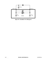
The oscillator circuit is designed for applications using a crystal or ceramic resonator
operating from 1 MHz to 20 MHz. The bias resistor and small startup capacitors are
integrated into the oscillator circuit, shown in Figure 5-2. Depending on the crystal and
application, an additional external capacitor may be required (consult crystal vendor for
specific information). The following equation can be used to calculate the size of external
capacitance:
C
L
= C
P
+
C
IN
Χ
C
OUT
C
IN
+ C
OUT
Where:
C
P
is the parasitic capacitance, which can be neglected in most cases.
C
IN
is the total input capacitance, consisting of C
ext
+ C1.
C
OUT
is the total output capacitance, consisting of C2 and external parasitic
capacitances (e.g., board and package capacitances).


