6- 18
MC68306 USER'S MANUAL
MOTOROLA
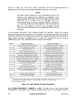
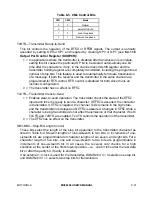
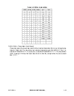
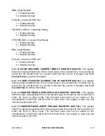
shown in Figure 6-9. The mode, status, command, and clock-select registers are
duplicated for each channel to provide independent operation and control.
NOTE
All serial module registers are only accessible as bytes. The
contents of the mode registers (DUMR1 and DUMR2), clock-
select register (DUCSR), and the auxiliary control register
(DUACR) bit 7 should only be changed after the
receiver/transmitter is issued a software RESET command—
i.e., channel operation must be disabled. Care should also be
taken if the register contents are changed during
receiver/transmitter operations, as undesirable results may be
produced.
In the registers discussed in the following pages, the numbers above the register
description represent the bit position in the register. The register description contains the
mnemonic for the bit. The values shown below the register description are the values of
those register bits after a hardware reset. A value of U indicates that the bit value is
unaffected by reset. The read/write status is shown in the last line.
Address
Register Read (R/W = 1)
Register Write (R/W = 0)
FFFFF7E1
MODE REGISTER A (DUMR1A, DUMR2A)
MODE REGISTER A (DUMR1A, DUMR2A)
FFFFF7E3
STATUS REGISTER A (DUSRA)
CLOCK-SELECT REGISTER A (DUCSRA)
FFFFF7E5
DO NOT ACCESS1
COMMAND REGISTER A (DUCRA)
FFFFF7E7
RECEIVER BUFFER A (DURBA)
TRANSMITTER BUFFER A (DUTBA)
FFFFF7E9
INPUT PORT CHANGE REGISTER (DUIPCR)
AUXILIARY CONTROL REGISTER (DUACR)
FFFFF7EB
INTERRUPT STATUS REGISTER (DUISR)
INTERRUPT MASK REGISTER (DUIMR)
FFFFF7ED
COUNTER MODE:CURRENT MSB OF COUNTER
COUNTER/TIMER UPPER REGISTER
FFFFF7EF
COUNTER MODE:CURRENT LSB OF COUNTER
COUNTER/TIMER LOWER REGISTER
FFFFF7F1
MODE REGISTER B (DUMR1B, DUMR2B)
MODE REGISTER B (DUMR1B, DUMR2B)
FFFFF7F3
STATUS REGISTER B (DUSRB)
CLOCK-SELECT REGISTER B (DUCSRB)
FFFFF7F5
DO NOT ACCESS1
COMMAND REGISTER B (DUCRB)
FFFFF7F7
RECEIVER BUFFER B (DURBB)
TRANSMITTER BUFFER B (DUTBB)
FFFFF7F9
INTERRUPT VECTOR REGISTER (DUIVR)
INTERRUPT VECTOR REGISTER (DUIVR)
FFFFF7FB
INPUT PORT REGISTER (DUIP)
OUTPUT PORT CONFIGURATION REGISTER
(DUOPCR)
FFFFF7FD
START COUNTER COMMAND2
OUTPUT PORT (DUOP) 2 BIT SET
FFFFF7FF
STOP COUNTER COMMAND2
OUTPUT PORT (DUOP) 2 BIT RESET
NOTES:
1. This address is used for factory testing and should not be read. Reading this location wiill result in undesired effects and
possible incorrect transmission or reception of characters. Register contents may also be changed.
2. Address-triggered commands
Figure 6-9. Serial Module Programming Model
6.4.1.1 MODE REGISTER 1 (DUMR1). DUMR1 controls some of the serial module
configuration. This register can be read or written at any time. It is accessed when the


