background image

MOTOROLA

MC68306 USER'S MANUAL

3- 31

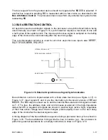
AS

R/W

DTACK

UDS/LDS

DATA

ADDR

Figure 3-28 Fully Asynchronous Read Cycle

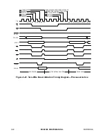
ADDR

AS

R/W

UDS/LDS

DATA

DTACK

Figure 3-29. Fully Asynchronous Write Cycle

In the asynchronous mode, the accessed device operates independently of the frequency
and phase of the system clock. For example, the MC68681 dual universal asynchronous
receiver/transmitter (DUART) does not require any clock-related information from the bus
master during a bus transfer. Asynchronous devices are designed to operate correctly
with processors at any clock frequency when relevant timing requirements are observed.

A device can use a clock at the same frequency as the system clock (e.g., 8, 10, or 12.5
MHz), but without a defined phase relationship to the system clock. This mode of
operation is pseudo-asynchronous; it increases performance by observing timing
parameters related to the system clock frequency without being completely synchronous
with that clock. A memory array designed to operate with a particular frequency processor
but not driven by the processor clock is a common example of a pseudo-asynchronous
device.

The designer of a fully asynchronous system can make no assumptions about address
setup time, which could be used to improve performance. With the system clock frequency
known, the slave device can be designed to decode the address bus before recognizing
an address strobe. Parameter #11 (refer to AC Electrical Specifications—Read and
Write Cycles
) specifies the minimum time before address strobe during which the
address is valid.

Summary of Contents for MC68306

Page 1: ...torola products are not designed intended or authorized for use as components in systems intended for surgical implant into the body or other applications intended to support or sustain life or for any other application in which the failure of the Motorola product could create a situation where personal injury or death may occur Should Buyer purchase or use Motorola products for any such unintende...

Page 2: ...7 IEEE 1149 1 Test Access Port Section 8 Electrical Specifications Section 9 Ordering Information and Mechanical Data 68K FAX IT Documentation Comments FAX 512 891 8593 Documentation Comments Only The Motorola High End Technical Publications Department provides a fax number for you to submit any questions or comments about this document or how to order other documents We welcome your suggestions f...

Page 3: ...ONTARIO Ottawa 613 226 3491 QUEBEC Montreal 514 731 6881 INTERNATIONAL AUSTRALIA Melbourne 61 3 887 0711 AUSTRALIA Sydney 61 2 906 3855 BRAZIL Sao Paulo 55 11 815 4200 CHINA Beijing 86 505 2180 FINLAND Helsinki 358 0 35161191 Car Phone 358 49 211501 FRANCE Paris Vanves 33 1 40 955 900 GERMANY Langenhagen Hanover 49 511 789911 GERMANY Munich 49 89 92103 0 GERMANY Nuremberg 49 911 64 3044 GERMANY Si...

Page 4: ...Signal Descriptions 2 1 Bus Signals 2 5 2 1 1 Address Bus A23 A1 2 5 2 1 2 Address Strobe AS 2 5 2 1 3 Bus Error BERR 2 5 2 1 4 Bus Request BR 2 5 2 1 5 Bus Grant BG 2 6 2 1 6 Bus Grant Acknowledge BGACK 2 6 2 1 7 Data Bus D15 D0 2 6 2 1 8 Data Transfer Acknowledge DTACK 2 6 2 1 9 DRAM Multiplexed Address Bus DRAMA14 DRAMA0 2 6 2 1 10 Processor Function Codes FC2 FC0 2 6 2 1 11 Halt HALT 2 7 2 1 1...

Page 5: ...ress Mode AMODE 2 10 2 6 Serial Module Signals 2 10 2 6 1 Channel A Receiver Serial Data Input RxDA 2 10 2 6 2 Channel A Transmitter Serial Data Output TxDA 2 10 2 6 3 Channel B Receiver Serial Data Input RxDB 2 10 2 6 4 Channel B Transmitter Serial Data Output TxDB 2 10 2 6 5 CTSA 2 11 2 6 6 RTSA 2 11 2 6 7 CTSB 2 11 2 6 8 RTSB 2 11 2 6 9 Crystal Oscillator X1 X2 2 11 2 6 10 IP2 2 11 2 6 11 OP3 2...

Page 6: ...ation 3 30 3 8 Synchronous Operation 3 33 Section 4 EC000 Core Processor 4 1 Features 4 1 4 2 Processing States 4 1 4 3 Programming Model 4 2 4 3 1 Data Format Summary 4 3 4 3 2 Addressing Capabilities Summary 4 4 4 3 3 Notation Conventions 4 5 4 4 EC000 Core Instruction Set Overview 4 7 4 5 Exception Processing 4 12 4 5 1 Exception Vectors 4 14 4 6 Processing of Specific Exceptions 4 16 4 6 1 Res...

Page 7: ...7 DRAM Control Registers 5 12 5 2 7 1 DRAM Refresh Register 5 13 5 2 7 2 DRAM Bank Configuration Register High Half 5 14 5 2 7 3 DRAM Bank Configuration Register Low Half 5 14 5 2 8 Automatic DTACK Generation 5 16 5 3 Crystal Oscillator 5 16 Section 6 Serial Module 6 1 Module Overview 6 2 6 1 1 Serial Communication Channels A and B 6 3 6 1 2 Baud Rate Generator Logic 6 3 6 1 3 Timer Counter 6 3 6 ...

Page 8: ...unter Mode 6 16 6 3 5 2 Timer Mode 6 16 6 3 6 Bus Operation 6 17 6 3 6 1 Read Cycles 6 17 6 3 6 2 Write Cycles 6 17 6 3 6 3 Interrupt Acknowledge Cycles 6 17 6 4 Register Description and Programming 6 17 6 4 1 Register Description 6 17 6 4 1 1 Mode Register 1 DUMR1 6 18 6 4 1 2 Mode Register 2 DUMR2 6 20 6 4 1 3 Status Register DUSR 6 22 6 4 1 4 Clock Select Register DUCSR 6 24 6 4 1 5 Command Reg...

Page 9: ... 3 7 4 Instruction Register 7 9 7 4 1 EXTEST 000 7 10 7 4 2 SAMPLE PRELOAD 110 7 10 7 4 3 BYPASS 010 101 111 7 11 7 4 4 CLAMP 011 7 11 7 5 MC68306 Restrictions 7 11 7 6 Non IEEE 1149 1 Operation 7 12 Section 8 Electrical Specifications 8 1 Maximum Ratings 8 1 8 2 Thermal Characteristics 8 1 8 3 Power Considerations 8 2 8 4 AC Electrical Specification Definitions 8 2 8 5 DC Electrical Specification...

Page 10: ...l Characteristics Interrupt Reset 8 16 8 15 AC Electrical Characteristics Transmitter Timing 8 17 8 16 AC Electrical Characteristics Receiver Timing 8 18 8 17 IEEE 1149 1 Electrical Characteristics 8 19 Section 9 Ordering Information and Mechanical Data 9 1 Standard Ordering Information 9 1 9 2 Pin Assignments 9 2 ...

Page 11: ...ing Diagram 3 15 Figure 3 15 Two Wire Bus Arbitration Timing Diagram 3 15 Figure 3 16 External Asynchronous Signal Synchronization 3 17 Figure 3 17 Bus Arbitration Unit State Diagrams 3 19 Figure 3 18 Three Wire Bus Arbitration Timing Diagram Processor Active 3 20 Figure 3 19 Three Wire Bus Arbitration Timing Diagram Bus Inactive 3 21 Figure 3 20 Three Wire Bus Arbitration Timing Diagram Special C...

Page 12: ...nctional Diagram 6 14 Figure 6 8 Multidrop Mode Timing Diagram 6 15 Figure 6 9 Serial Module Programming Model 6 18 Figure 6 10 Serial Module Programming Flowchart 6 38 Figure 7 1 Test Access Port Block Diagram 7 2 Figure 7 2 TAP Controller State Machine 7 3 Figure 7 3 Output Cell O Cell 7 7 Figure 7 4 Input Cell I Cell 7 7 Figure 7 5 Output Control Cell En Cell 7 8 Figure 7 6 Bidirectional Cell I...

Page 13: ...it Test and Set 8 15 Figure 8 12 Clock Timing 8 16 Figure 8 13 Port Timing 8 16 Figure 8 14 Interrupt Reset Timing 8 17 Figure 8 15 Transmit Timing 8 17 Figure 8 16 Receive Timing 8 18 Figure 8 17 Test Clock Input Timing Diagram 8 19 Figure 8 18 Boundary Scan Timing Diagram 8 20 Figure 8 19 Test Access Port Timing Diagram 8 20 ...

Page 14: ...3 25 Table 4 1 Processor Data Formats 4 3 Table 4 2 Effective Addressing Modes 4 4 Table 4 3 Notation Conventions 4 5 Table 4 4 EC000 Core Instruction Set Summary 4 8 Table 4 5 Exception Vector Assignments 4 16 Table 4 6 Exception Grouping and Priority 4 22 Table 5 1 MC68306 Memory Map 5 2 Table 5 2 Chip Select Match Bits 5 11 Table 5 3 DRAM Address Multiplexer 5 13 Table 5 4 DRAM Bank Match Bits ...

Page 15: ...vi MC68306 USER S MANUAL MOTOROLA LIST OF TABLES Continued Table Page Number Title Number Table 7 1 Boundary Scan Control Bits 7 4 Table 7 2 Boundary Scan Bit Definitions 7 5 Table 7 3 Instructions 7 10 ...

Page 16: ...mic random access memory DRAM can especially benefit from using the MC68306 The MC68306 s high level of functional integration results in significant reductions in component count power consumption board space and cost while yielding much higher system reliability and shorter design time Complete code compatibility with the MC68000 affords the designer access to a broad base of established real ti...

Page 17: ...rupt Controller Bus Timeout 24 Address Lines 16 Data Lines 16 67 MHz 5 Volt Operation 144 Pin Thin Quad Flat Pack TQFP or 132 Pin Plastic Quad Flat Pack PQFP 1 1 MC68EC000 CORE PROCESSOR The MC68EC000 is a core implementation of the MC68000 32 bit microprocessor architecture The programmer can use any of the eight 32 bit data registers for fast manipulation of data and any of the eight 32 bit addr...

Page 18: ...tor terminals or remote devices The MC68306 contains a two channel full duplex UART with an integrated timer An on chip baud rate generator provides standard baud rates up the 38 4K baud to each channel s receiver and transmitter The serial module is identical to the MC68681 MC2681 DUART Each communication channel is completely independent Data formats can be 5 6 7 or 8 bits with even odd or no pa...

Page 19: ...rammed After reset chip select CS0 responds to all accesses until the chip selects have been properly programmed Four of the chip selects are multiplexed with the most significant address bits A23 A20 The address mode AMODE input determines the functions of these outputs 1 2 4 Parallel Ports Two 8 bit parallel ports are provided The port pins can be individually programmed to be inputs or outputs ...

Page 20: ...ically terminate and report as erroneous any bus cycle that is not normally terminated after a pre programmed length of time The user can program this timeout period to be up to 4096 clocks 1 2 8 IEEE 1149 1 Test To aid in system diagnostics the MC68306 includes dedicated user accessible test logic that is fully compliant with the IEEE 1149 1 standard for boundary scan testability often referred t...

Page 21: ...ovides a quick reference for determining a signal s name mnemonic its use as an input or output active state and type identification NOTE The terms assertion and negation will be used extensively This is done to avoid confusion when dealing with a mixture of active low and active high signals The term assert or assertion is used to indicate that a signal is active or true independent of whether th...

Page 22: ...S TDI TDO PA7 PA6 PA5 PA4 PA3 PA2 PA1 PA0 DRAM CONTROLLER INTERRUPT CONTROLLER MODE CONTROLLER CTSB IP1 CTSA IP0 CS0 CS1 CS2 CS3 CS4 A20 CS5 A21 CS6 A22 CS7 A23 PORT B CHIP SELECTS AMODE RAS1 RAS0 CAS1 IRQ7 IRQ4 IRQ1 IACK7 IACK4 IACK1 A15 DRAMA14 A1 DRAMA0 CAS0 IRQ6 PB7 IRQ5 PB6 IRQ3 PB5 IRQ2 PB4 IACK6 PB3 IACK5 PB2 IACK3 PB1 IACK2 PB0 TRST LDS UW LW DTACK DRAMW OE CLOCK IP2 16 BIT TIMER COUNTER O...

Page 23: ...robe UDS I O Yes 4 7 K Lower Byte Write Strobe LW Output No Upper Byte Write Strobe UW Output No Output Enable OE Output No Read Write R W Output Yes Reset RESET I O 2 2 K NOTES 1 Pullup may be required value depends on individual application Must not be left floating Table 2 2 Chip Select Signal Summary Signal Name Mnemonic Input Output Three State During Bus Arbitration Pullup Required Chip Sele...

Page 24: ...O 2 Interrupt Acknowledge 7 4 1 IACK7 IACK4 IACK1 Output Interrupt Acknowledge 6 Port B 7 IACK6 PB3 I O 2 Interrupt Acknowledge 5 Port B 6 IACK5 PB2 I O 2 Interrupt Acknowledge 3 Port B 5 IACK3 PB1 I O 2 Interrupt Acknowledge 2 Port B 4 IACK2 PB0 I O 2 Port A PA7 PA0 I O 2 NOTES 2 Pullup or pulldown may be required value depends on individual application Table 2 5 Clock and Mode Control Signal Sum...

Page 25: ...lup may be required value depends on individual application Must not be left floating Table 2 7 JTAG Signal Summary Signal Name Mnemonic Input Output Three State During Bus Arbitration Pulldown Required Test Clock TCK Input Test Data Input TDI Input Test Data Output TDO Output Test Mode Select TMS Input Test Reset TRST Input 4 7 K 3 NOTES 3 Pin has internal pullup but external pulldown may be requ...

Page 26: ...een the bus error signal and the halt signal 2 1 4 Bus Request BR This input can be wire ORed with bus request signals from all other devices that could be bus masters Assertion of this signal indicates to the processor that some other device needs to become the bus master Bus requests can be issued at any time during a bus cycle or between cycles 2 1 5 Bus Grant BG This output signal indicates to...

Page 27: ...for any chip select cycle Refer to 3 7 Asynchronous Operation and 3 8 Synchronous Operation 2 1 9 DRAM Multiplexed Address Bus DRAMA14 DRAMA0 These signals provide fifteen multiplexed address bits used during row address strobe 2 1 10 Processor Function Codes FC2 FC0 These function code outputs indicate the mode user or supervisor and the address space type currently being accessed as shown in Tab...

Page 28: ... the processor drives the data bus When another bus master controls the bus the UDS LDS and R W pins become inputs and the OE LW and UW signals are still decoded as shown in Table 2 9 Table 2 9 Data Strobe Control of Data Bus UDS LDS R W D8 D15 D0 D7 OE UW LW High High No Valid Data No Valid Data High High High Low Low High Valid Data Bits 15 8 Valid Data Bits 7 0 Low High High High Low High No Va...

Page 29: ...rnal state of the processor The interaction of internal and external RESET and the HALT signal is described in paragraph 3 5 Reset Operation 2 2 CHIP SELECT SIGNALS These eight three state signals provide address decodes with programmable base and range CS7 CS4 are only available in chip select mode AMODE bit 1 CS3 CS0 are always available 2 3 DRAM CONTROLLER SIGNALS The following signals are used...

Page 30: ...programmed to serve as port B parallel input output signals 2 5 CLOCK AND MODE CONTROL SIGNALS These four pins are used to connect an external crystal to the on chip oscillator and define the four multifunction pins 2 5 1 Crystal Oscillator EXTAL XTAL These two pins are the connections for an external crystal to the internal oscillator circuit If an external oscillator is used it should be connect...

Page 31: ...a Output TxDB This signal is the transmitter serial data output for channel B The least significant bit is transmitted first This output is held high mark condition when the transmitter is disabled idle or operating in the local loopback mode Data is shifted out of this pin on the falling edge of the programmed clock source 2 6 5 CTSA This input can be used as the channel A clear to send active lo...

Page 32: ...nnel B transmitter 1X clock output or the channel B receiver 1X clock output 2 7 JTAG PORT TEST SIGNALS The following signals are used with the on chip test logic defined by the IEEE 1149 1 standard See IEEE 1149 1 Test Access Port for more information on the use of these signals 2 7 1 Test Clock TCK This input provides a clock for on chip test logic defined by the IEEE 1149 1 standard 2 7 2 Test ...

Page 33: ...e In all cases the bus master must deskew all signals it issues at both the start and end of a bus cycle In addition the bus master must deskew the acknowledge and data signals from the slave device The following paragraphs describe the read write read modify write and CPU space cycles The indivisible read modify write cycle implements interlocked multiprocessor communications A CPU space cycle is...

Page 34: ... CYCLE OUTPUT THE DATA 1 DECODE ADDRESS 2 PLACE DATA ON D15 D0 3 ASSERT DATA TRANSFER ACKNOWLEDGE DTACK 1 REMOVE DATA FROM D15 D0 2 NEGATE DTACK SLAVE START NEXT CYCLE Figure 3 1 Word Read Cycle Flowchart BUS MASTER ADDRESS THE DEVICE 1 SET R W TO READ 2 PLACE FUNCTION CODE ON FC2 FC0 3 PLACE ADDRESS ON ADDRESS BUS 4 ASSERT ADDRESS STROBE AS 5 ASSERT UPPER DATA STROBE UDS OR LOWER DATA STROBE LDS ...

Page 35: ...1 A1 AS UDS LDS R W DTACK D15 D8 D7 D0 READ WRITE 2 WAIT STATE READ Figure 3 3 Read and Write Cycle Timing Diagram S0 S1 S2 S3 S4 S5 S6 S7 S0 S1 S2 S3 S4 S5 S6 S7 S0 S1 S2 S3 S4 S5 S6 S7 Internal Signal Only CLK FC2 FC0 A31 A1 AS UDS LDS R W DTACK D15 D8 D7 D0 READ WRITE READ A0 Figure 3 4 Word and Byte Read Cycle Timing Diagram ...

Page 36: ...s signals are altered STATE 6 Sometime between state 2 S2 and state 6 S6 data from the device is driven onto the data bus STATE 7 On the falling edge of the clock entering state 7 S7 the processor latches data from the addressed device and negates AS and UDS LDS The device negates DTACK or BERR at this time Case 2 BERR received without DTACK STATE 5 During state 5 S5 no bus signals are altered STA...

Page 37: ...ER ADDRESS THE DEVICE 1 PLACE FUNCTION CODE ON FC2 FC0 2 PLACE ADDRESS ON ADDRESS BUS 3 ASSERT ADDRESS STROBE AS 4 SET R W TO WRITE 5 PLACE DATA ON D15 D0 6 ASSERT UPPER DATA STROBE UDS AND LOWER DATA STROBE LDS TERMINATE THE CYCLE INPUT THE DATA 1 DECODE ADDRESS 2 LATCH DATA ON D15 D0 3 ASSERT DATA TRANSFER ACKNOWLEDGE DTACK SLAVE START NEXT CYCLE 1 NEGATE DTACK TERMINATE OUTPUT TRANSFER 1 NEGATE...

Page 38: ...FROM D7 D0 OR D15 D8 4 SET R W TO READ TERMINATE THE CYCLE INPUT THE DATA 1 DECODE ADDRESS 2 LATCH DATA ON D7 D0 IF LDS IS ASSERTED LATCH DATA ON D15 D8 IF UDS IS ASSERTED 3 ASSERT DATA TRANSFER ACKNOWLEDGE DTACK SLAVE START NEXT CYCLE TERMINATE OUTPUT TRANSFER 1 NEGATE DTACK Figure 3 6 Byte Write Cycle Flowchart S0 S1 S2 S3 S4 S5 S6 S7 S0 S1 S2 S3 S4 S5 S6 S7 S0 S1 S2 S3 S4 S5 S6 S7 INTERNAL SIGN...

Page 39: ... altered STATE 6 During S6 no bus signals are altered STATE 7 On the falling edge of the clock entering S7 the processor negates AS UDS and or LDS As the clock rises at the end of S7 the processor places the data bus in the high impedance state and drives R W high The device negates DTACK or BERR at this time Case 2 BERR received without DTACK STATE 5 During state 5 S5 no bus signals are altered S...

Page 40: ...E OUTPUT THE DATA 1 DECODE ADDRESS 2 PLACE DATA ON D7 D0 OR D15 D0 3 ASSERT DATA TRANSFER ACKNOWLEDGE DTACK SLAVE START NEXT CYCLE 1 REMOVE DATA FROM D7 D0 OR D15 D8 2 NEGATE DTACK 1 LATCH DATA 1 NEGATE UDS AND LDS 2 START DATA MODIFICATION ACQUIRE THE DATA START OUTPUT TRANSFER 1 SET R W TO WRITE 2 PLACE DATA ON D7 D0 OR D15 D8 3 ASSERT UPPER DATA STROBE UDS OR LOWER DATA STROBE LDS TERMINATE OUT...

Page 41: ...ocessor asserts AS and UDS LDS STATE 3 During S3 no bus signals are altered STATE 4 During S4 the processor waits for a cycle termination signal DTACK or BERR If neither termination signal is asserted before the falling edge at the end of S4 the processor inserts wait states full clock cycles until either DTACK or BERR is asserted Case R1 DTACK only STATE 5 During S5 no bus signals are altered STA...

Page 42: ...thout BERR STATE 17 During S17 no bus signals are altered STATE 18 During S18 no bus signals are altered STATE 19 On the falling edge of the clock entering S19 the processor negates AS and UDS LDS As the clock rises at the end of S19 the processor places the data bus in the high impedance state and drives R W high The device negates DTACK or BERR at this time Case R2 DTACK and BERR on read STATE 5...

Page 43: ... core CPU space is used only for interrupt acknowledge cycles Figure 3 10 shows the encoding of an interrupt acknowledge cycle 1 1 1 1 1 1 1 1 1 1 1 1 1 1 1 1 1 1 1 1 1 1 1 1 1 1 1 1 1 1 1 INTERRUPT ACKNOWLEDGE 31 LEVEL 1 3 1 0 Figure 3 10 Interrupt Acknowledge Cycle The interrupt acknowledge cycle places the level of the interrupt being acknowledged on address bits A3 A1 and drives all other addr...

Page 44: ...SITION IPL2 IPL0 SAMPLED IPL2 IPL0 VALID INTERNALLY SW SW IACK Figure 3 11 Interrupt Acknowledge Cycle Timing Diagram 3 2 BUS ARBITRATION Bus arbitration is a technique used by bus master devices to request to be granted and to acknowledge bus mastership Bus arbitration consists of the following 1 Asserting a bus mastership request 2 Receiving a grant indicating that the bus is available at the en...

Page 45: ...TRATION DETER MINES NEXT BUS MASTER 2 NEXT BUS MASTER WAITS FOR CURRENT CYCLE TO COMPLETE 3 NEXT BUS MASTER ASSERTS BUS GRANT ACKNOWLEDGE BGACK TO BECOME NEW MASTER 4 BUS MASTER NEGATES BR TERMINATE ARBITRATION 1 NEGATE BGACK PROCESSOR 1 ASSERT BUS GRANT BG ACKNOWLEDGE BUS MASTERSHIP OPERATE AS BUS MASTER 1 PERFORM DATA TRANSFERS READ AND WRITE CYCLES ACCORDING TO THE SAME RULES THE PRO CESSOR USE...

Page 46: ...BR PROCESSOR 1 ASSERT BUS GRANT BG OPERATE AS BUS MASTER REARBITRATE OR RESUME PROCESSOR OPERATION RELEASE BUS MASTERSHIP ACKNOWLEDGE RELEASE OF BUS MASTERSHIP 1 NEGATE BUS GRANT BG 1 EXTERNAL ARBITRATION DETER MINES NEXT BUS MASTER 2 NEXT BUS MASTER WAITS FOR CURRENT CYCLE TO COMPLETE Figure 3 13 Two Wire Bus Arbitration Cycle Flowchart ...

Page 47: ...BGACK PROCESSOR DMA DEVICE PROCESSOR DMA DEVICE Figure 3 14 Three Wire Bus Arbitration Timing Diagram CLK FC2 FC0 A19 A0 AS DS R W DTACK D7 D0 PROCESSOR BR BG S0 S6 S2 S4 S0 S2 S4 S6 S0 S2 S4 S6 S0 S2 S4 S6 DMA DEVICE PROCESSOR DMA DEVICE Figure 3 15 Two Wire Bus Arbitration Timing Diagram ...

Page 48: ... open collector devices from any of the devices in the system that can become bus master The processor which is at a lower bus priority level than the external devices relinquishes the bus after it completes the current bus cycle 3 2 2 Receiving the Bus Grant The processor asserts BG as soon as possible Normally this process immediately follows internal synchronization except when the processor ha...

Page 49: ...L2 IPL0 CLK BR EXTERNAL BR iNTERNAL 47 INTERNAL SIGNAL VALID EXTERNAL SIGNAL SAMPLED Figure 3 16 External Asynchronous Signal Synchronization Bus arbitration control is implemented with a finite state machine see Figure 3 17 In Figure 3 17 input signals R and A are the internally synchronized versions of BR and BGACK The BG output is shown as G and the internal three state control signal is shown ...

Page 50: ...XA RA RX 1 1 R Bus Request Internal A Bus Grant Acknowledge Internal G Bus Grant T Three state Control to Bus Control Logic X Don t Care Notes 1 State machine will not change if the bus is S0 or S1 Refer to 5 2 3 BUS ARBITRATION CONTROL 2 The address bus will be placed in the high impedance state if T is asserted and AS is negated R R R X R X R R a 3 Wire Bus Arbitration b 2 Wire Bus Arbitration G...

Page 51: ... S4 S5 S6 S7 S0 S1 S2 S3 S4 S5 S6 S7 S0 S1 CLK BUS THREE STATED BG ASSERTED BR VALID INTERNAL BR SAMPLED BR ASSERTED BUS RELEASED FROM THREE STATE AND PROCESSOR STARTS NEXT BUS CYCLE BGACK NEGATED INTERNAL BGACK SAMPLED BGACK NEGATED BR BG BGACK FC2 FC0 A31 A1 AS UDS LDS R W DTACK D15 D0 PROCESSOR ALTERNATE BUS MASTER PROCESSOR Figure 3 18 Three Wire Bus Arbitration Timing Diagram Processor Active...

Page 52: ...D AND BUS THREE STATED BR VALID INTERNAL BR SAMPLED BR ASSERTED BR BG BGACK FC2 FC0 A31 A1 AS UDS LDS R W DTACK D15 D0 BUS RELEASED FROM THREE STATE AND PROCESSOR STARTS NEXT BUS CYCLE PROCESSOR PROCESSOR BUS INACTIVE ALTERNATE BUS MASTER Figure 3 19 Three Wire Bus Arbitration Timing Diagram Bus Inactive ...

Page 53: ...US RELEASED FROM THREE STATE AND PROCESSOR STARTS NEXT BUS CYCLE BGACK NEGATED INTERNAL BGACK SAMPLED BGACK NEGATED BR BG BGACK AS UDS LDS R W DTACK D15 D0 S0 S2 S4 S6 S0 S2 S4 S6 S0 CLK FC2 FC0 A31 A1 PROCESSOR ALTERNATE BUS MASTER PROCESSOR Figure 3 20 Three Wire Bus Arbitration Timing Diagram Special Case ...

Page 54: ...ERTED BR VALID INTERNAL BR SAMPLED BR ASSERTED BUS RELEASED FROM THREE STATE AND PROCESSOR STARTS NEXT BUS CYCLE BR NEGATED INTERNAL BR SAMPLED BR NEGATED BR BG BGACK FC2 FC0 A31 A1 AS UDS LDS R W DTACK D15 D0 PROCESSOR ALTERNATE BUS MASTER PROCESSOR Figure 3 21 Two Wire Bus Arbitration Timing Diagram Processor Active ...

Page 55: ... AND BUS THREE STATED BR VALID INTERNAL BR SAMPLED BR ASSERTED BR BG BGACK FC2 FC0 A31 A1 AS UDS LDS R W DTACK D15 D0 BUS RELEASED FROM THREE STATE AND PROCESSOR STARTS NEXT BUS CYCLE PROCESSOR PROCESSOR BUS INACTIVE ALTERNATE BUS MASTER Figure 3 22 Two Wire Bus Arbitration Timing Diagram Bus Inactive ...

Page 56: ...rror input is provided to terminate a bus cycle in error when the expected signal is not asserted Different systems and different devices within the same system require different maximum response times External circuitry can be provided to assert the bus error signal after the appropriate delay following the assertion of address strobe 3 4 1 Bus Error Operation A bus error is recognized when BERR ...

Page 57: ...register 2 Program counter two words which may be up to five words past the instruction being executed 3 Error information The first two items are identical to the information stacked by any other exception The EC000 core stacks bus error information to help determine and to correct the error After the processor has placed the required information on the stack the bus error exception vector is rea...

Page 58: ...d that the write portion of the operation is performed without negating the address strobe the processor does not retry a read modify write cycle When BERR occurs during a read modify write operation a bus error operation is performed whether or not HALT is asserted 3 4 3 Halt Operation HALT performs a halt run single step operation When HALT is asserted by an external device the processor halts a...

Page 59: ... processing by stacking information on the supervisor stack If another bus error occurs during exception processing i e before execution of another instruction begins the processor halts and asserts HALT This is called a double bus fault Only an external reset operation can restart a processor halted due to a double bus fault A retry operation does not initiate exception processing a bus error dur...

Page 60: ...ld reset all external devices the EC000 core itself is not affected The processor drives RESET for 124 clock periods The RESET signal is asserted by an external source to reset the EC000 core RESET by itself will reset the EC000 core unless the processor is executing a RESET instruction To guarantee a reset of the core RESET must be asserted for at least 132 clocks i e longer than the maximum dura...

Page 61: ...LT Assertion Results Case No Control Signal Asserted on Rising Edge of State EC000 Core Results N N 2 1 DTACK BERR HALT A NA NA S NA X Normal cycle terminate and continue 2 DTACK BERR HALT A NA A S S NA S Normal cycle terminate and halt Continue when HALT negated 3 DTACK BERR HALT X A NA X S NA Terminate and take bus error trap 4 DTACK BERR HALT A NA NA S A NA Normal cycle terminate and continue 5...

Page 62: ...s bus error trap Rerun BERR HALT or Illegal sequence usually traps to vector number 0 Rerun BERR HALT Reruns the bus cycle Normal BERR HALT or May lengthen next cycle Normal BERR HALT or none If next cycle is started it will be terminated as a bus error Signal is negated in this bus state 3 7 ASYNCHRONOUS OPERATION To achieve clock frequency independence at a system level the bus can be operated i...

Page 63: ...clock e g 8 10 or 12 5 MHz but without a defined phase relationship to the system clock This mode of operation is pseudo asynchronous it increases performance by observing timing parameters related to the system clock frequency without being completely synchronous with that clock A memory array designed to operate with a particular frequency processor but not driven by the processor clock is a com...

Page 64: ...pecifies the minimum time between the transition of R W and the driving of the data bus which is effectively the maximum turnoff time for any device driving the data bus After the processor places valid data on the bus it asserts the data strobe signal s A data setup time similar to the address setup time previously discussed can be used to improve performance Parameter 26 is the minimum time a sl...

Page 65: ...e consists of four clock periods eight bus cycle states and optionally an integral number of clock cycles inserted as wait states Wait states are inserted as required to allow sufficient response time for the external device The following state by state description of the bus cycle differs from those descriptions in 3 1 1 Read Cycle and 3 1 2 Write Cycle by including information about the importan...

Page 66: ...owledged by the processor If either DTACK or BERR is asserted before the falling edge of S4 and satisfies the input setup time defined by parameter 47 the processor enters S5 and the bus cycle continues If either DTACK or BERR is asserted but without meeting the setup time defined by parameter 47 the processor may recognize the signal and continue the bus cycle the result is unpredictable If neith...

Page 67: ...R W high External logic circuitry should respond to the negation of the AS and UDS LDS by negating DTACK and or BERR Parameter 28 is the hold time for DTACK and parameter 30 is the hold time for BERR Figure 3 32 shows a synchronous read cycle and the important timing parameters that apply The timing for a synchronous read cycle including relevant timing parameters is shown in Figure 3 33 ADDR UDS ...

Page 68: ...nization requires that the internal machine receives a valid logic level whether the input is high low or in transition Parameter 47 of AC Electrical Specifications Read and Write Cycles is the asynchronous input setup time Signals that meet parameter 47 are guaranteed to be recognized at the next falling edge of the system clock However signals that do not meet parameter 47 are not guaranteed to ...

Page 69: ...eption vector stacking operations and refilling the instruction pipe after an exception The processor enters exception processing when an exceptional internal condition arises such as tracing an instruction an instruction results in a trap or executing specific instructions External conditions such as interrupts and access errors also cause exceptions Exception processing ends when the first instr...

Page 70: ...ter and an 8 bit condition code register The first eight registers D0 D7 are used as data registers for byte 8 bit word 16 bit and long word 32 bit operations The second set of seven registers A0 A6 and the user stack pointer USP can be used as software stack pointers and base address registers In addition the address registers can be used for word and long word operations All of the 16 registers ...

Page 71: ...M68000 family The instruction set supports operations on other data formats such as memory addresses The operand data formats supported by the integer unit IU are the standard twos complement data formats defined in the M68000 family architecture Registers memory or instructions themselves can contain IU operands The operand size for each instruction is either explicitly encoded in the instruction...

Page 72: ...e addressing mode for an operand These instructions include the appropriate fields for operands that use only one addressing mode Table 4 2 lists a summary of the effective addressing modes for the processor Refer to M68000PM AD M68000 Family Programmer s Reference Manual for details on instruction format and addressing modes Table 4 2 Effective Addressing Modes Addressing Modes Syntax Register Di...

Page 73: ...OP Enter the stopped state waiting for interrupts operand 10 The operand is BCD operations are performed in decimal If condition then operations else operations Test the condition If true the operations after then are performed If the condition is false and the optional else clause is present the operations after else are performed If the condition is false and else is omitted the instruction perf...

Page 74: ...e instruction word s Identifies an indirect address in a register Identifies an indirect address in memory bd Base Displacement dn Displacement Value n Bits Wide example d16 is a 16 bit displacement LSB Least Significant Bit LSW Least Significant Word MSB Most Significant Bit MSW Most Significant Word od Outer Displacement SCALE A scale factor 1 2 4 or 8 for no word word long word or quad word sca...

Page 75: ...ign of the instruction set gives special emphasis to support of structured high level languages and to ease of assembly language programming Each instruction with a few exceptions operates on bytes words and long words and most instructions can use any of the 14 addressing modes Over 1000 useful instructions are provided by combining instruction types data types and addressing modes These instruct...

Page 76: ...NDI data CCR ANDI to SR If supervisor state then Source Λ SR SR else TRAP ANDI data SR ASL ASR Destination Shifted by count Destination ASd Dx Dy1 ASd data Dy1 ASd ea 1 Bcc If condition true then PC dn PC Bcc label BCHG bit number of Destination Z bit number of Destination bit number of Destination BCHG Dn ea BCHG data ea BCLR bit number of Destination Z 0 bit number of Destination BCLR Dn ea BCLR...

Page 77: ...rce CCR CCR EORI data CCR EORI to SR If supervisor state then Source SR SR else TRAP EORI data SR EXG Rx Ry EXG Dx Dy EXG Ax Ay EXG Dx Ay EXG Ay Dx EXT Destination Sign Extended Destination EXT W Dn extend byte to word EXT L Dn extend word to long word JMP Destination Address PC JMP ea JSR SP 4 SP PC SP Destination Address PC JSR ea LEA ea An LEA ea An LINK SP 4 SP An SP SP An SP d SP LINK An dn L...

Page 78: ...NEG 0 Destination Destination NEG ea NEGX 0 Destination X Destination NEGX ea NOP None NOP NOT Destination Destination NOT ea OR Source V Destination Destination OR ea Dn OR Dn ea ORI Immediate Data V Destination Destination ORI data ea ORI to CCR Source V CCR CCR ORI data CCR ORI to SR If supervisor state then Source V SR SR else TRAP ORI data SR PEA SP 4 SP ea SP PEA ea RESET If supervisor state...

Page 79: ...nation Source Destination SUBA ea An SUBI Destination Immediate Data Destination SUBI data ea SUBQ Destination Immediate Data Destination SUBQ data ea SUBX Destination Source X Destination SUBX Dx Dy SUBX Ax Ay SWAP Register 31 16 Register 15 0 SWAP Dn TAS Destination Tested Condition Codes 1 bit 7 of Destination TAS ea TRAP SSP 2 SSP Format Offset SSP SSP 4 SSP PC SSP SSP 2 SSP SR SSP Vector Addr...

Page 80: ...rivilege violations cause exceptions Exception processing uses an exception vector table and an exception stack frame Exception processing occurs in four functional steps However all individual bus cycles associated with exception processing vector acquisition stacking etc are not guaranteed to occur in the order in which they are described in this section Figure 4 3 illustrates a general flowchar...

Page 81: ...ULT DOUBLE BUS FAULT ENTRY SAVE CONTENTS TO STACK FRAME SEE NOTE OTHERWISE BEGIN INSTRUCTION EXECUTION OTHERWISE BUS ERROR BUS ERROR BUS ERROR OR ADDRESS ERROR OTHERWISE SAVE INTERNAL COPY OF SR S 1 T 0 SEE NOTE NOTE These blocks vary for reset and interrupt exceptions EC28 Figure 4 3 General Exception Processing Flowchart ...

Page 82: ...coding and execution is started 4 5 1 Exception Vectors An exception vector is a memory location from which the processor fetches the address of a routine to handle an exception Each exception type requires a handler routine and a unique vector All exception vectors are two words in length see Figure 4 5 except for the reset vector which is four words long All exception vectors reside in the super...

Page 83: ... bus of the particular implementation of the M68000 architecture In the EC000 core this is 24 address bits The memory map for exception vectors is shown in Table 4 5 The vector table is 512 words long 1024 bytes starting at address 0 decimal and proceeding through address 1023 decimal The vector table provides 255 unique vectors some of which are reserved for trap and other system function vectors...

Page 84: ...r 28 29 30 31 070 074 078 07C SD SD SD SD Level 4 Interrupt Autovector Level 5 Interrupt Autovector Level 6 Interrupt Autovector Level 7 Interrupt Autovector 32 47 080 0BC SD TRAP 0 15 Instruction Vectors4 48 631 0C0 0FC Unassigned Reserved 64 255 100 3FC SD User Defined Vectors NOTES 1 Vector numbers 12 13 16 23 and 48 63 are reserved for future enhancements by Motorola No user peripheral devices...

Page 85: ...upt priority and interrupts are inhibited for all priority levels less than or equal to the current priority Priority level 7 is a special case Level 7 interrupts cannot be inhibited by the interrupt priority mask thus providing a non maskable interrupt capability An interrupt is generated each time the interrupt request level changes from some lower level to level 7 A level 7 interrupt may still ...

Page 86: ...sing 4 6 5 Instruction Traps Traps are exceptions caused by instructions they occur when a processor recognizes an abnormal condition during instruction execution or when an instruction is executed that normally traps during execution Exception processing for traps is straightforward The status register is copied the supervisor mode is entered and tracing is turned off The vector number is interna...

Page 87: ...s AND Immediate to SR MOVE USP EOR Immediate to SR OR Immediate to SR MOVE to SR RESET MOVE from SR RTE MOVEC STOP MOVES Exception processing for privilege violations is nearly identical to that for illegal instructions After the instruction is fetched and decoded and the processor determines that a privilege violation is being attempted the processor starts exception processing The status registe...

Page 88: ...g is terminated and the processor immediately begins exception processing Exception processing for a bus error follows the usual sequence of steps The status register is copied the supervisor mode is entered and tracing is turned off The vector number is generated to refer to the bus error vector Since the processor is fetching the instruction or an operand when the error occurs the context of the...

Page 89: ...ror An address error exception occurs when the processor attempts to access a word or long word operand or an instruction at an odd address An address error is similar to an internally generated bus error The bus cycle is aborted and the processor ceases current processing and begins exception processing The exception processing sequence is the same as that for a bus error including the informatio...

Page 90: ...ng a TRAP instruction the bus error takes precedence and the TRAP instruction processing is aborted In another example if an interrupt request occurs during the execution of an instruction while the T bit in the status register SR is asserted the trace exception has priority and is processed first Before instruction execution resumes however the interrupt exception is also processed and instructio...

Page 91: ...he internal EC000 core The effect of the RESET instruction and external assertion of the hardware RESET signal on MC68306 components is External RESET RESET Instruction EC000 Core Yes No Serial Module Yes Yes MC68306 Registers See Individual Descriptions No 5 1 MC68306 ADDRESS SPACE The full 32 bit address capability of the MC68306 corresponding to a 4 Gbyte address space is decoded internally A s...

Page 92: ... 6 CONFIGURATION HIGH 5 FFFFFFD6 FFFFFFD4 CHIP SELECT 5 CONFIGURATION LOW CHIP SELECT 5 CONFIGURATION HIGH 5 FFFFFFD2 FFFFFFD0 CHIP SELECT 4 CONFIGURATION LOW CHIP SELECT 4 CONFIGURATION HIGH 5 FFFFFFCE FFFFFFCC CHIP SELECT 3 CONFIGURATION LOW CHIP SELECT 3 CONFIGURATION HIGH 5 FFFFFFCA FFFFFFC8 CHIP SELECT 2 CONFIGURATION LOW CHIP SELECT 2 CONFIGURATION HIGH 5 FFFFFFC6 FFFFFFC4 CHIP SELECT 1 CONF...

Page 93: ...reset is the value of the AMODE pin latched at reset FFFFFFFE 15 14 13 12 11 10 9 8 BTERR BTEN 0 AMOD E 0 DUIPL 2 DUIPL 1 DUIPL 0 RESET 0 0 0 AMOD E 0 1 0 0 SUPERVISOR ONLY BTERR Bus Timeout Error This bit is read only and is cleared when read Writes to this bit are ignored 0 No bus timeout bus error 1 Bus timeout bus error occurred BTEN Bus Timeout Enable This bit is used to enable the bus timeou...

Page 94: ...imer Vector The value set in this field supplies the vector for the DUART timer interrupt handler 5 2 3 Bus Timeout Period Register FFFFFFFC 7 6 5 4 3 2 1 0 BT7 BT6 BT5 BT4 BT3 BT2 BT1 BT0 RESE T U U U U U U U U SUPERVISOR ONLY A programmable period timer can generate a bus error to terminate any bus cycle after 16 to 4096 wait states programmable in 16 wait state increments The bus timeout timer ...

Page 95: ...pt control register Auto vectored interrupt acknowledge cycles are zero wait states If no active interrupt is present at the level being acknowledged the MC68306 automatically generates a spurious interrupt vector which is a zero wait state Interrupt input synchronization is frozen during an interrupt acknowledge cycle so the acknowledge can safely be used to automatically negate the interrupt 5 2...

Page 96: ...icates the DUART interrupt state 0 No DUART interrupt 1 DUART interrupt asserted IX7 1 Reset inactive level of external interrupts 7 through 1 0 Active high interrupt pin 1 Active low interrupt pin 5 2 5 I O Port Registers The following paragraphs describe the registers controlling the parallel ports All port pins are reset to input by a system reset so pullup or pulldown resistors should be added...

Page 97: ...e interrupt is open drain or open source The active interrupt level is the inverse of the IX register bit 5 2 5 1 PORT PINS REGISTER FFFFFFF4 5 15 14 13 12 11 10 9 8 7 6 5 4 3 2 1 0 PA7 PA6 PA5 PA4 PA3 PA2 PA1 PA0 PB7 PB6 PB5 PB4 PB3 PB2 PB1 PB0 RESE T PA7 PA6 PA5 PA4 PA3 PA2 PA1 PA0 PB7 PB6 PB5 PB4 PB3 PB2 PB1 PB0 SUPERVISOR ONLY The port pin register bits are the data at the port pins regardless...

Page 98: ...re separate chip select pulses for the read and write portions of a read modify write cycle The four mask bits CSM3 CSM0 are decoded to an n of 15 mask where n is the binary value of CSM3 CSM0 On every bus cycle the n most significant address bits of the range A31 A17 are compared and the remaining less significant bits are ignored The fifteen address bits are first masked by each chip select mask...

Page 99: ...e address range and cycle duration of each chip select to be independently programmed The chip select configuration registers do not support byte writes The registers can be written as either 16 bit or 32 bit but 32 bit accesses are preferred Any write access affects all 16 bits of the high half or low half register Only chip select 0 is affected by reset 5 2 6 1 CHIP SELECT CONFIGURATION REGISTER...

Page 100: ...LY CSR Chip Select Read This bit determines whether read cycles are permitted to chip select space If read and write cycles are both inhibited chip select is inhibited 0 Read cycles are inhibited to chip select space 1 Read cycles are permitted to chip select space CSFC 6 5 2 1 Chip Select Function Code Enable This bit determines which function code accesses are permitted to chip select space If a...

Page 101: ...field determines whether automatic DTACK is returned and how many wait states are inserted if automatic DTACK is enabled When automatic DTACK is selected the write portion of a TAS indivisible cycle is the same length as a normal write cycle to the same location Any external DTACK generation circuit must recognize that AS remains asserted throughout a read write indivisible cycle if it supports TA...

Page 102: ...th bytes are refreshed together The refresh timer is not affected by any reset and refresh cycles will appear under reset The refresh timer is initialized by a write to the refresh rate register When this register is written the first refresh occurs immediately so the refresh rate should be programmed after the DRAM configuration register DRDT bit After power up the refresh rate register value is ...

Page 103: ...the address multiplexer shown in Table 5 3 Table 5 3 DRAM Address Multiplexer Value Of At RAS When DRSZ2 0 Is At CAS 111 110 101 100 011 010 001 000 DRAMA14 A30 A29 A28 A27 A26 A25 A24 A23 A15 DRAMA13 A29 A28 A27 A26 A25 A24 A23 A22 A14 DRAMA12 A28 A27 A26 A25 A24 A23 A22 A21 A13 DRAMA11 A27 A26 A25 A24 A23 A22 A21 A20 A12 DRAMA10 A26 A25 A24 A23 A22 A21 A20 A19 A11 DRAMA9 A25 A24 A23 A22 A21 A20 ...

Page 104: ...uration registers are not affected by any reset and must be explicitly programmed This applies to both banks whether used or not Unused banks must be disabled to prevent interference with other address decodes FFFFFFE4 5 DR1 FFFFFFE0 1 DR0 15 14 13 12 11 10 9 8 7 6 5 4 3 2 1 0 DRA31 DRA3 0 DRA2 9 DRA2 8 DRA2 7 DRA2 6 DRA2 5 DRA2 4 DRA2 3 DRA2 2 DRA21 DRA20 DRA19 DRA18 DRA1 7 DRW RESE T U U U U U U...

Page 105: ...which function code accesses are permitted to DRAM bank space If all function code cycles are inhibited the DRAM bank is inhibited 0 Function code n cycles are inhibited to DRAM bank space 1 Function code n cycles are permitted to DRAM bank space DRM3 0 DRAM Bank Address Match This field determines which DRAM bank address bits must match address bits for DRAM bank to occur DRA bits not included in...

Page 106: ... 1100 x x x 1101 x x 1110 x 1111 x Address bit is a don t care DRA bit must be 0 to allow match Address bit must match DRA bit for DRAM bank to occur DRSZ DRAM Size DRAM address multiplexer provides 8 DRSZ2 0 CAS address bits NOTE Both DRAM banks must be the same size and speed The DRAM logic uses the DRSZ and DRDT values programmed in the bank 0 configuration register only These bits in the bank ...

Page 107: ...hat AS remains asserted throughout a read write indivisible cycle if it supports TAS For the DRAM address spaces the write portion of a TAS is always 0 wait regardless of DRDT 5 3 CRYSTAL OSCILLATOR The oscillator circuit is designed for applications using a crystal or ceramic resonator operating from 1 MHz to 20 MHz The bias resistor and small startup capacitors are integrated into the oscillator...

Page 108: ...5 18 MC68306 USER S MANUAL MOTOROLA C1 15 pf C2 12 pf EXTAL X1 XTAL X2 CEXT MC68306 10 M Figure 5 2 Oscillator Circuit Diagram ...

Page 109: ...s of the following major functional areas Two Independent Serial Communication Channels A and B Baud Rate Generator Logic Sixteen Bit Timer Counter Internal Channel Control Logic Interrupt Control Logic SERIAL COMMUNICATIONS CHANNELS A AND B BAUD RATE GENERATOR LOGIC INTERNAL CHANNEL CONTROL LOGIC X1 CLK X2 INTERRUPT CONTROL LOGIC RxDB RxDA TxDB TxDA IP0 IP1 IP2 OP0 OP1 OP3 16 BIT TIMER COUNTER Fi...

Page 110: ...ammable in One Sixteenth Bit Increments Programmable Channel Modes Normal Full Duplex Automatic Echo Local Loopback Remote Loopback Automatic Wakeup Mode for Multidrop Applications Multi Function Three Bit Input Port Can Be Clock or Control Inputs Change of State Detection Available Multi Function Three Bit Output Port Individual Bit Set Reset Capability Can Be Status or Interrupt Signal Multi Fun...

Page 111: ...he baud rate generator operates from the oscillator or external CMOS clock input and is capable of generating 18 commonly used data communication baud rates ranging from 50 to 38 4k by producing internal clock outputs at 16 times the actual baud rate Refer to 6 2 Serial Module Signal Definitions and 6 3 1 Baud Rate Generator for additional information 6 1 3 Timer Counter The timer counter provides...

Page 112: ...and active high signals The term assert or assertion indicates that a signal is active or true independent of the level represented by a high or low voltage The term negate or negation indicates that a signal is inactive or false 6 2 1 Crystal Input or External Clock X1 CLK This input is one of two connections to a crystal or a single connection to an external clock A crystal or an external clock ...

Page 113: ...e 6 2 External and Internal Interface Signals 6 2 4 Channel A Receiver Serial Data Input RxDA This signal is the receiver serial data input for channel A Data received on this signal is sampled on the rising edge of the clock source with the least significant bit received first 6 2 5 Channel B Transmitter Serial Data Output TxDB This signal is the transmitter serial data output for channel B The o...

Page 114: ...o send or as a dedicated parallel output 6 2 8 1 RTSB When used for this function this signal can be programmed to be automatically negated and asserted by either the receiver or transmitter When connected to the CTS input of a transmitter this signal can be used to control serial data flow 6 2 8 2 OP1 When used for this function this output is controlled by bit 1 in the DUOP register 6 2 9 Channe...

Page 115: ...nal clock of the same frequency Baud rates are selected by programming the clock select register DUCSR for each channel BAUD RATE GENERATOR LOGIC CRYSTAL OSCILLATOR BAUD RATE GENERATOR CLOCK SELECTORS X1 X2 EXTERNAL INTERFACE Figure 6 3 Baud Rate Generator Block Diagram 6 3 2 Transmitter and Receiver Operating Modes The functional block diagram of the transmitter and receiver including command and...

Page 116: ...MODE REGISTER 1 MR1A MODE REGISTER 2 MR2A STATUS REGISTER SRA W R W R W R EXTERNAL INTERFACE RECEIVER HOLDING REGISTER 1 RECEIVER HOLDING REGISTER 2 RECEIVER HOLDING REGISTER 3 RECEIVER SHIFT REGISTER TxDB RxDB FIFO TRANSMIT HOLDING REGISTER TRANSMIT SHIFT REGISTER RECEIVE BUFFER RBB 4 REGISTERS W R COMMAND REGISTER CRB MODE REGISTER 1 MR1B MODE REGISTER 2 MR2B STATUS REGISTER SRB W R W R W R TRAN...

Page 117: ... is shifted from the transmitter output on the falling edge of the clock source C1 C2 C3 C4 C6 W W W W W W W W C1 C2 C3 C4 STOP BREAK START BREAK C5 NOT TRANSMITTED C6 BREAK C1 IN TRANSMISSION TxDx TRANSMITTER ENABLED TxRDY SR2 CS CTS IP0 RTS OP0 2 1 NOTES 1 TIMING SHOWN FOR MR2 4 1 2 TIMING SHOWN FOR MR2 5 1 3 C TRANSMIT CHARACTER 4 W WRITE N MANUALLY ASSERTED BY BIT SET COMMAND MANUALLY ASSERTED...

Page 118: ...When a transition is detected the state of RxDx is sampled each 16 clock for eight clocks starting one half clock after the transition asynchronous operation or at the next rising edge of the bit time clock synchronous operation If RxDx is sampled high the start bit is invalid and the search for the valid start bit begins again If RxDx is still low a valid start bit is assumed and the receiver con...

Page 119: ...n the break begins in the middle of a character the receiver places the damaged character in the receiver first in first out FIFO stack and sets the corresponding error conditions and RxRDY bit in the DUSR Then if the break persists until the next character time the receiver places an all zero character into the receiver FIFO and sets the corresponding RB and RxRDY bits in the DUSR 6 3 2 3 FIFO ST...

Page 120: ...s performed at the end of the message This mode allows a data reception speed advantage but does have a disadvantage since each character is not individually checked for error conditions by software If an error occurs within the message the error is not recognized until the final check is performed and no indication exists as to which character in the message is at fault In either mode reading the...

Page 121: ...framing is also checked but stop bits are transmitted as received A received break is echoed as received until the next valid start bit is detected 6 3 3 2 LOCAL LOOPBACK MODE In this mode TxDx is internally connected to RxDx This mode is useful for testing the operation of a local serial module channel by sending data to the transmitter and checking data assembled by the receiver In this manner c...

Page 122: ... an address character followed by a block of data characters targeted for one of the slave stations The slave stations have their channel receivers disabled However they continuously monitor the data stream sent out by the master station When an address character is sent by the master the slave receiver channel notifies its respective CPU by setting the RxRDY bit in the DUSR and generating an inte...

Page 123: ...on The character is interpreted as an address character if the A D bit is set or as a data character if the A D bit is cleared The polarity of the A D bit is selected by programming bit 2 of the DUMR1 The DUMR1 should be programmed before enabling the transmitter and loading the corresponding data bits into the transmit buffer In multidrop mode the receiver continuously monitors the received data ...

Page 124: ...mer operates in counter mode 6 3 5 1 COUNTER MODE In the counter mode the counter timer counts down from the preload value using the programmed counter clock source The counter clock source can be the X1 CLK pin the channel A transmitter clock the channel B transmitter clock or an external clock on the input port pin IP2 The CPU can start and stop the counter and can read the count value DUCUR DUC...

Page 125: ...ad write and interrupt acknowledge cycles to the serial module All serial module registers must be accessed as bytes 6 3 6 1 READ CYCLES The serial module is accessed by the CPU with a variable number of wait states depending on the relative phase of the CPU and serial module clocks The maximum number of wait states for a 16 67 MHz CPU clock and 3 6864 MHz serial module clock is six The serial mod...

Page 126: ...SRA CLOCK SELECT REGISTER A DUCSRA FFFFF7E5 DO NOT ACCESS1 COMMAND REGISTER A DUCRA FFFFF7E7 RECEIVER BUFFER A DURBA TRANSMITTER BUFFER A DUTBA FFFFF7E9 INPUT PORT CHANGE REGISTER DUIPCR AUXILIARY CONTROL REGISTER DUACR FFFFF7EB INTERRUPT STATUS REGISTER DUISR INTERRUPT MASK REGISTER DUIMR FFFFF7ED COUNTER MODE CURRENT MSB OF COUNTER COUNTER TIMER UPPER REGISTER FFFFF7EF COUNTER MODE CURRENT LSB O...

Page 127: ...de Register 2 for information on programming the transmitter RTS control RxIRQ Receiver Interrupt Select 1 FFULL is the source that generates IRQ 0 RxRDY is the source that generates IRQ ERR Error Mode This bit controls the meaning of the three FIFO status bits RB FE and PE in the DUSR for the channel 1 Block mode The values in the channel DUSR are the accumulation i e the logical OR of the status...

Page 128: ...a Character 1 1 Multidrop Mode 1 Address Character B C1 B C0 Bits per Character These bits select the number of data bits per character to be transmitted The character length listed in Table 6 2 does not include start parity or stop bits Table 6 2 B Cx Control Bits B C1 B C0 Bits Character 0 0 Five Bits 0 1 Six Bits 1 0 Seven Bits 1 1 Eight Bits 6 4 1 2 MODE REGISTER 2 DUMR2 DUMR2 controls some of...

Page 129: ...ear to send operation The transmitter checks the state of the CTS input each time it is ready to send a character If CTS is asserted the character is transmitted If CTS is negated the channel TxDx remains in the high state and the transmission is delayed until CTS is asserted Changes in CTS while a character is being transmitted do not affect transmission of that character If both TxCTS and TxRTS ...

Page 130: ... 5 4 3 2 1 0 RB FE PE OE TxEMP TxRDY FFULL RxRDY RESET 0 0 0 0 0 0 0 0 Read Only RB Received Break 1 An all zero character of the programmed length has been received without a stop bit The RB bit is only valid when the RxRDY bit is set Only a single FIFO position is occupied when a break is received Further entries to the FIFO are inhibited until the channel RxDx returns to the high state for at l...

Page 131: ...command in the DUCR 0 No overrun has occurred TxEMP Transmitter Empty 1 The channel transmitter has underrun both the transmitter holding register and transmitter shift registers are empty This bit is set after transmission of the last stop bit of a character if there are no characters in the transmitter holding register awaiting transmission 0 The transmitter buffer is not empty Either a characte...

Page 132: ...el receiver and transmitter DUCSRA DUCSRB 7 6 5 4 3 2 1 0 RCS3 RCS2 RCS1 RCS0 TCS3 TCS2 TCS1 TCS0 RESET 0 0 0 0 0 0 0 0 Write Only RCS3 RCS0 Receiver Clock Select These bits select the baud rate clock for the channel receiver from a set of baud rates listed in Table 6 5 The baud rate set selected depends upon the auxiliary control register DUACR bit 7 Set 1 is selected if DUACR bit 7 0 and set 2 i...

Page 133: ...1 0 7200 1800 1 0 1 1 9600 9600 1 1 0 0 38 4k 19 2k 1 1 0 1 TIMER TIMER 1 1 1 0 1 1 1 1 TCS3 TCS0 Transmitter Clock Select These bits select the baud rate clock for the channel transmitter from a set of baud rates listed in Table 6 6 The baud rate set selected depends upon DUACR bit 7 Set 1 is selected if DUACR bit 7 0 and set 2 is selected if DUACR bit 7 1 The transmitter clock is always 16 times...

Page 134: ...38 4k 19 2k 1 1 0 1 TIMER TIMER 1 1 1 0 1 1 1 1 6 4 1 5 COMMAND REGISTER DUCR The DUCR is used to supply commands to the channel Multiple commands can be specified in a single write to the DUCR if the commands are not conflicting e g reset transmitter and enable transmitter commands cannot be specified in a single command DUCRA DUCRB 7 6 5 4 3 2 1 0 MISC2 MISC1 MISC0 TC1 TC0 RC1 RC0 RESET 0 0 0 0 ...

Page 135: ... command whenever the transmitter configuration is changed because it places the transmitter in a known state Reset Error Status The reset error status command clears the channel s RB FE PE and OE bits in the DUSR This command is also used in the block mode to clear all error bits after a data block is received Reset Break Change Interrupt The reset break change interrupt command clears the delta ...

Page 136: ...ve If the transmitter is already disabled this command has no effect Do Not Use Do not use this bit combination because the result is indeterminate RC1 RC0 Receiver Commands These bits select a single command as listed in Table 6 9 Table 6 9 RCx Control Bits RC1 RC0 Command 0 0 No Action Taken 0 1 Enable Receiver 1 0 Disable Receiver 1 1 Do Not Use No Action Taken The no action taken command cause...

Page 137: ...ansmitter holding register and the transmitter shift register see Figure 6 4 The holding register accepts characters from the bus master if the TxRDY bit in the channel s DUSR is set A write to the transmitter buffer clears the TxRDY bit inhibiting any more characters until the shift register is ready to accept more data When the shift register is empty it checks to see if the holding register has...

Page 138: ...ll be set which will initiate an interrupt if the corresponding IECx bit of the DUACR register is enabled 1 The current state of the respective IPx input is logic one negated if used as CTS 0 The current state of the respective IPx input is logic zero asserted if used as CTS 6 4 1 9 AUXILIARY CONTROL REGISTER DUACR The DUACR selects which baud rate is used and controls the handshake of the transmi...

Page 139: ...bit in the DUIPCR has no effect on DUISR bit 7 6 4 1 10 INTERRUPT STATUS REGISTER DUISR The DUISR provides status for all potential interrupt sources The contents of this register are masked by the DUIMR If a flag in the DUISR is set and the corresponding bit in DUIMR is also set the IRQ output is asserted If the corresponding bit in the DUIMR is cleared the state of the bit in the DUISR has no ef...

Page 140: ...holding register when TxRDYx 0 are not transmitted CTR TMR_RDY Counter Timer Ready 1 Counter timer ready 0 Counter timer not ready DBA Delta Break A See DBB RxRDYA Channel A Receiver Ready or FIFO Full See RxRDYB The function of this bit is programmed by DUMR1A bit 6 TxRDYA Channel A Transmitter Ready See TxRDYB This bit is the duplication of the TxRDY bit in DUSRA 6 4 1 11 INTERRUPT MASK REGISTER...

Page 141: ...ENT LSB OF COUNTER DUCLR This register holds the least significant byte of the current value in the counter timer It should only be read when the counter timer is in counter mode and the counter is stopped See 6 3 5 Counter Timerfor further information 6 4 1 14 COUNTER TIMER UPPER PRELOAD REGISTER DUCTUR This register holds the eight most significant bits of the preload value to be used by the con...

Page 142: ... information 6 4 1 17 INPUT PORT REGISTER The DUIP register shows the current state of the IPx inputs DUIP 7 6 5 4 3 2 1 0 1 1 IP5 IP4 IP3 IP2 IP1 IP0 1 1 1 1 1 IP2 IP1 IP0 Read Only IP5 IP4 IP3 IP2 IP1 IP0 Current State 1 The current state of the respective IP input is logic one 0 The current state of the respective IP input is logic zero The information contained in these bits is latched and ref...

Page 143: ...and 2 are not pinned out on the MC68306 thus changing bits 7 6 5 4 1 and 0 of this register has no effect OPCR3 OPCR2 Output Port 3 Function Select 00 OPR bit 3 01 Counter timer output 10 TxCB 1X 11 RxCB 1X NOTE OP3 is open drain in this mode and an external pullup is required OPCR1 OPCR0 Output Port 2 Function Select 00 OPR bit 2 01 TxCA 16X 10 TxCA 1X 11 RxCA 1X ...

Page 144: ...esponding to one bits on the data bus 0 These bits are not affected by writing a zero to this address Bit Reset DUOP 7 6 5 4 3 2 1 0 OP7 OP6 OP5 OP4 OP3 OP2 OP1 OP0 RESET 0 0 0 0 0 0 0 0 Write Only OP3 OP1 OP0 Output Port Parallel Outputs 1 A write cycle to the OP bit reset command address clears all OP bits corresponding to one bits on the data bus 0 These bits are not affected by writing a zero ...

Page 145: ...ceivers and transmitters are enabled The CHCHK routine performs the actual channel checks as called from the SINIT routine When called SINIT places the specified channel in the local loopback mode and checks for the following errors Transmitter Never Ready Receiver Never Ready Parity Error Incorrect Character Received 6 4 2 2 I O DRIVER EXAMPLE The I O driver routines consist of INCH and OUTCH INC...

Page 146: ...EL A STATUS POINT TO CHANNEL B SAVE CHANNEL B STATUS ANY ERRORS IN CHANNEL A ENABLE CHANNEL A S RECEIVER ASSERT CHANNEL A REQUEST TO SEND ANY ERRORS IN CHANNEL B ENABLE CHANNEL B S TRANSMITTER RETURN SINIT CHK1 CHK2 ENABLA Y N ENABLB SINITR CALL CHCHK CALL CHCHK Y N Figure 6 10 Serial Module Programming Flowchart 1 of 5 ...

Page 147: ...MITTER CLEAR CHANNEL STATUS WORD IS TRANSMITTER READY WAITED TOO LONG WAITED TOO LONG N Y SEND CHARACTER TO TRANSMITTER HAS RECEIVER RECEIVED CHARACTER CHCHK TxCHK SNDCHR RxCHK N Y N SET TRANSMITTER NEVER READY FLAG SET RECEIVER NEVER READY FLAG A B Y Figure 6 10 Serial Module Programming Flowchart 2 of 5 ...

Page 148: ...RAMING ERROR FLAG HAVE PARITY ERROR SET PARITY ERROR FLAG GET CHARACTER FROM RECEIVER SAME AS CHARACTER TRANSMITTED SET INCORRECT CHARACTER FLAG DISABLE CHANNEL S TRANSMITTER RESTORE CHANNEL TO ORIGINAL MODE FRCHK RSTCHN PRCHK CHRCHK Figure 6 10 Serial Module Programming Flowchart 3 of 5 ...

Page 149: ...Qx ARRIVED YET CLEAR CHANGE IN BREAK STATUS BIT REMOVE BREAK CHARACTER FROM RECEIVER FIFO REPLACE RETURN ADDRESS ON SYSTEM STACK AND MONITOR WARM START ADDRESS RTE SIRQR N Y N DOES CHANNEL A RECEIVER HAVE A CHARACTER SAVE IN SYSTEM BUFFER N Y ABRKI1 ABRKI Y INCH RETURN SIRQ Figure 6 10 Serial Module Programming Flowchart 4 of 5 ...

Page 150: ...6 42 MC68306 USER S MANUAL MOTOROLA OUTCH N Y IS CHANNEL TRANSMITTER READY SEND CHARACTER TO CHANNEL TRANSMITTER RETURN Figure 6 10 Serial Module Programming Flowchart 5 of 5 ...

Page 151: ...rupt sources Auxiliary Control Register DUACR Select baud rate set BRG bit Initialize the input enable control IEC bits Select counter timer mode and clock source if necessary Output Port Control Register DUOPCR Select the function of the output port pins The following steps are channel specific Clock Select Register DUCSR Select the receiver and transmitter clock Mode Register 1 DUMR1 If desired ...

Page 152: ...6 44 MC68306 USER S MANUAL MOTOROLA If desired program operation of clear to send TxCTS bit Select stop bit length SBx bits Command Register DUCR Enable the receiver and transmitter ...

Page 153: ... is independent of the device system logic The MC68306 implementation provides the following capabilities a Perform boundary scan operations to test circuit board electrical continuity b Sample the MC68306 system pins during operation and transparently shift out the result in the boundary scan register c Bypass the MC68306 for a given circuit board test by effectively reducing the boundary scan re...

Page 154: ...K test clock input to synchronize the test logic with pulldown TMS test mode select input with an internal pullup resistor that is sampled on the rising edge of TCK to sequence the TAP controller s state machine TDI test data input with an internal pullup resistor that is sampled on the rising edge of TCK TDO three state test data output that is actively driven in the shift IR and shift DR control...

Page 155: ... the TCK signal For a description of the TAP controller states please refer to the IEEE 1149 1 document TEST LOGIC RESET RUN TEST IDLE SELECT DR_SCAN CAPTURE DR SELECT IR_SCAN CAPTURE IR SHIFT DR SHIFT IR EXIT1 DR EXIT1 IR PAUSE DR PAUSE IR EXIT2 DR UPDATE DR EXIT2 IR UPDATE IR 1 0 1 1 0 1 0 0 1 0 1 0 0 1 1 1 0 0 1 0 1 1 1 0 1 1 0 0 0 0 0 1 Figure 7 2 TAP Controller State Machine 7 3 BOUNDARY SCAN...

Page 156: ... PPOE5 38 CSOE 100 PPOE14 24 PPOE6 40 AOE 118 Boundary scan bit definitions are shown in Table 7 2 The first column in Table 7 2 defines the bit s ordinal position in the boundary scan register The shift register bit nearest TDO i e first to be shifted out is defined as bit 0 the last bit to be shifted out is bit 123 The second column references one of the five MC68306 cell types depicted in Figur...

Page 157: ... IACK7 HiZ 13 IO Cell PA0 PPOE8 47 I Cell IRQ1 14 En Cell PPOE9 48 I Cell IRQ4 15 IO Cell PA1 PPOE9 49 I Cell IRQ7 16 En Cell PPOE10 50 IO Cell D0 DOE 17 IO Cell PA2 PPOE10 51 IO Cell D1 DOE 18 En Cell PPOE11 52 IO Cell D2 DOE 19 IO Cell PA3 PPOE11 53 IO Cell D3 DOE 20 En Cell PPOE12 54 IO Cell D4 DOE 21 IO Cell PA4 PPOE12 55 IO Cell D5 DOE 22 En Cell PPOE13 56 IO Cell D6 DOE 23 IO Cell PA5 PPOE13...

Page 158: ...GACK 106 IO Cell A4 DRAMA3 CPMOE 79 IO Cell AS CPMOE 107 IO Cell A5 DRAMA4 CPMOE 80 IO Cell R W CPMOE 108 IO Cell A6 DRAMA5 CPMOE 81 IO Cell UDS CPMOE 109 IO Cell A7 DRAMA6 CPMOE 82 IO Cell LDS CPMOE 110 IO Cell A8 DRAMA7 CPMOE 83 O Cell UW HiZ 111 IO Cell A9 DRAMA8 CPMOE 84 O Cell LW HiZ 112 IO Cell A10 DRAMA9 CPMOE 85 O Cell OE HiZ 113 IO Cell A11 DRAMA10 CPMOE 86 En Cell DRAMWOE 114 IO Cell A12...

Page 159: ...CELL 1 D C1 CLOCK DR 1 D C1 UPDATE DR SHIFT DR TO NEXT CELL TO OUTPUT BUFFER 1 EXTEST 0 OTHERWISE DATA FROM SYSTEM LOGIC Figure 7 3 Output Cell O Cell FROM LAST CELL 1 MUX 1 G1 TO DEVICE LOGIC INPUT PIN SHIFT DR CLOCK DR 1D C1 TO NEXT CELL Figure 7 4 Input Cell I Cell ...

Page 160: ...PDATE DR TO NEXT CELL TO OUTPUT ENABLE 1 EXTEST 0 OTHERWISE SHIFT DR Figure 7 5 Output Control Cell En Cell 1 MUX 1 G1 1 MUX 1 G1 OUTPUT FROM SYSTEM LOGIC FROM LAST CELL 1D C1 CLOCK DR 1D C1 UPDATE DR TO NEXT CELL TO OUTPUT DRIVER 1 EXTEST 0 OTHERWISE SHIFT DR FROM PIN INPUT TO SYSTEM LOGIC Figure 7 6 Bidirectional Cell IO Cell ...

Page 161: ...ROM LAST CELL OUTPUT DATA INPUT DATA OUTPUT ENABLE I O PIN TO NEXT CELL NOTE More than one lO Cell could be serially connected and controlled by a single En Cell EN CELL Figure 7 8 General Arrangement for Bidirectional Pins 7 4 INSTRUCTION REGISTER The MC68306 IEEE 1149 1 implementation includes the three mandatory public instructions EXTEST SAMPLE PRELOAD and BYPASS the optional public ID instruc...

Page 162: ...d by this action since an update IR signal is required to modify them 7 4 1 EXTEST 000 The external test EXTEST instruction selects the 124 bit boundary scan register EXTEST asserts internal reset for the MC68306 system logic to force a predictable benign internal state while performing external boundary scan operations By using the TAP the register is capable of a scanning user defined values int...

Page 163: ... the bypass register is selected by the current instruction the shift register stage is set to a logic zero on the rising edge of TCK in the capture DR controller state Therefore the first bit to be shifted out after selecting the bypass register will always be a logic zero 7 4 4 CLAMP 011 When the CLAMP instruction is invoked the boundary scan multiplexer control signal EXTEST is asserted and the...

Page 164: ...pt transparent to the system logic by forcing the TAP controller into the test logic reset state This requires either 1 An active low signal applied to TRST 2 A minimum of five consecutive TCK rising edges withh TMS high TMS has an internal pullup and may be left unconnected If TMS either remains unconnected or is connected to VCC then the TAP controller cannot leave the test logic reset state reg...

Page 165: ...ltage1 2 Vin 0 3 to 7 0 V Operating Temperature Range TA 0 to 70 C Storage Temperature Range Tstg 55 to 150 C NOTES 1 Permanent damage can occur if maximum ratings are exceeded Exposure to voltages or currents in excess of recommended values affects device reliability Device modules may not operate normally while being exposed to electrical extremes 2 Although sections of the device contain circui...

Page 166: ...Equations 1 and 2 iteratively for any value of TA 8 4 AC ELECTRICAL SPECIFICATION DEFINITIONS The AC specifications presented consist of output delays input setup and hold times and signal skew times All signals are specified relative to an appropriate edge of the clock and possibly to one or more other signals The measurement of the AC specifications is defined by the waveforms shown in Figure 8 ...

Page 167: ...meters specified relative to the falling edge of the clock 3 This input timing is applicable to all parameters specified relative to the rising edge of the clock 4 This input timing is applicable to all parameters specified relative to the falling edge of the clock 5 This timing is applicable to all parameters specified relative to the assertion negation of another signal LEGEND A Maximum output d...

Page 168: ... Dissipation f 16 67 MHz PD 0 5 W Input Capacitance 3 All Input Only Pins All I O Pins Cin 10 20 pF Load Capacitance 3 CL 100 pF 1 Not including internal pullup or pulldown 2 Currents listed are with no loading 3 Capacitance is periodically sampled rather than 100 tested 8 6 AC ELECTRICAL SPECIFICATIONS CLOCK TIMING The electrical specifications in this document are preliminary see Figure 8 2 Num ...

Page 169: ... Valid Row Address for DRAM Cycle 30 ns 6A CLKOUT High to FC Valid 30 ns 7 CLKOUT High to Data Bus High Impedance Maximum 50 ns 8 CLKOUT High to Address FC Invalid Minimum 0 ns 91 CLKOUT High to AS LDS UDS Asserted 3 30 ns 9A UDS LDS Asserted to OE UW LW Asserted 0 15 ns 112 Address Valid to AS LDS UDS Asserted Read AS Asserted Write 15 ns 11A2 FC Valid to AS LDS UDS Asserted Read AS Asserted Writ...

Page 170: ...than or equal to 50 pF subtract 5 ns from the value given in the maximum columns 2 Actual value depends on clock period 3 If 47 is satisfied for both DTACK and BERR 48 may be ignored In the absence of DTACK BERR is an asynchronous input using the asynchronous input setup time 47 4 For power up the MC68306 must be held in the reset state for 100 ms to allow stabilization of on chip circuitry After ...

Page 171: ...RR BR NOTE 2 HALT RESET 47 ASYNCHRONOUS INPUTS NOTE 1 S7 31 11A NOTES 1 Setup time 47 for asynchronous inputs HALT RESET BR BGACK DTACK BERR IRQx guarantees their recognition at the next falling edge of the clock 2 BR need fall at this time only to ensure being recognized at the end of the bus cycle 9 15 OE 9A 12A 6 11 29A Figure 8 3 Read Cycle Timing Diagram ...

Page 172: ...11A 2 Because of loading variations R W may be valid after AS even though both are initiated by the rising edge of S2 specification 20A 14A 20A UW LW NOTES 1 Setup time 47 for asynchronous inputs HALT RESET BR BGACK DTACK BERR IRQx guarantees their recognition at the next falling edge of the clock 3 BR need fall at this time only to ensure being recognized at the end of the bus cycle NOTE 2 NOTE 2...

Page 173: ...valid 15 ns 66 CS Negated to R W Invalid 15 ns 67 Data Out Valid to CS Negated Write 90 ns 68 CS Negated to Data Out Invalid Write 15 ns 69 CS Negated to Data In High Impedance 90 ns 70 CLKOUT High to IACK Asserted 0 30 ns 70A LDS High to IACK Negated 0 10 ns V Boolean OR S0 S1 S2 S3 S4 S5 S6 CLKOUT FC2 FC0 A23 A0 AS R W DATA NOTE 1 LDS UDS CS S12 S13 S14 S15 S16 S17 S18 62 62 63 65 65 66 63 67 68...

Page 174: ...ed 40 ns 34 CLKOUT High to BG Negated 40 ns 35 BR Asserted to BG Asserted 1 5 6 5 Clks 36 BR Negated to BG Negated 1 5 3 5 Clks 37 BGACK Asserted to BG Negated 1 5 3 5 Clks 37A2 BGACK Asserted to BR Negated 20 ns 1 5 Clks 38 BG Asserted to Control Address Data Bus High Impedance AS Negated 50 ns 39 BG Width Negated 1 5 Clks 47 Asynchronous Input Setup Time 10 ns 57 BGACK Negated to Bus Driven 1 Cl...

Page 175: ... R W BR BGACK BG 35 33 38 34 39 46 37 37A 36 NOTE Setup time to the clock 47 for the asynchronous inputs BERR BGACK BR DTACK HALT RESET and IRQx guarantees their recognition at the next falling edge of the clock Figure 8 7 Bus Arbitration Timing Diagram ...

Page 176: ...ait State Operation 0 20 ns 85 CLKOUT High to CAS Asserted 1 Wait State Operation 0 20 ns 86 Column Address Valid to CAS Asserted 20 20 ns 87 CAS Asserted to Column Address Invalid 75 100 ns 88 CAS Width Asserted 60 90 90 120 ns 89 CLKOUT Low to RAS CAS Negated 0 30 0 30 ns 89A AS Negated to RAS CAS Negated 0 10 0 10 ns 90 CAS Width Negated Back to Back Cycles 150 180 ns 91 CAS Width Negated Page ...

Page 177: ...06 USER S MANUAL 8 13 CLKOUT FC0 FC2 D15 D0 A15 DRAMA 14 A1 DRAMA 0 AS UDS LDS R W UW LW OE DTACK DRAMW RAS CAS 71 73 74 75 78 88 81 76 80 82 84 86 87 90 71A 89A 89 80 90 Figure 8 8 DRAM Timing 0 Wait Read No Refresh ...

Page 178: ...W OE DTACK DRAMW RAS CAS 73 74 75 78 88 81 80 83 85 86 87 90 93 72 77 94 71A 89A 89 80 90 Figure 8 9 DRAM Timing 1 Wait Write No Refresh CLKOUT DRAMW RAS CAS 99 96 95 100 1 WAIT STATE 0 WAIT STATE 97 97 98 101 101 102 103 100 80 90 90 80 96 103 98 99 102 95 Figure 8 10 DRAM Timing 0 and 1 Wait Refresh ...

Page 179: ...er Timer Clock Frequency IP2 fCTC 0 16 67 MHz NOTES 1 All voltage measurements are referenced to ground GND For testing all input signals except X1 CLK swing between 0 4 V and 2 4 V with a maximum transition time of 20 ns For X1 CLK this swing is between 0 4 V and 4 4 V All time measurements are referenced at input and output voltages of 0 8 V and 2 0 V as appropriate Test conditions for outputs C...

Page 180: ...CLK tCTC tCLK tCTC X1 CLK IP2 FOR C T CLK Figure 8 12 Clock Timing 8 13 AC ELECTRICAL CHARACTERISTICS PORT TIMING See Figure 8 13 and Note Characteristic Symbol Min Max Unit Port Input Setup Time to LDS Asserted tPS 0 ns Port Input Hold Time from LDS Negated tPH 0 ns Port Output Valid from LDS Negated tPD 60 ns NOTE Test conditions for port outputs CL 50 pF RL 27 kΩ to VCC t PS LDS OP0 OP1 OP3 IP0...

Page 181: ... Interrupt Reset Timing 8 15 AC ELECTRICAL CHARACTERISTICS TRANSMITTER TIMING See Figure 8 15 and Note Characteristic Symbol Min Max Unit TxD Output Valid from TxC Low tTxD 100 ns CTS Input Setup to Tx Clock High tCS 30 ns CTS Input Hold from Tx Clock High tCH 30 ns RTS Output Valid from Tx Clock tTRD 100 ns CTS is an asynchronous input This specification is only provided to guarantee CTS recognit...

Page 182: ...ee Figure 8 16 and Note Characteristic Symbol Min Max Unit RxD Data Setup Time to RxC High tRxS 240 ns RxD Data Hold Time from RxC High tRxH 200 ns RTS Output Valid from Rx Clock tRRD 100 ns RxD Rx CLOCK SOURCE X1 OR IP2 tRxS tRxH OP0 OP1 t RRD When used as RxRTS Figure 8 16 Receive Timing ...

Page 183: ...Pulse Width Measured at 1 5 V 45 ns 3 TCK Rise and Fall Times 0 5 ns 6 Boundary Scan Input Data Setup Time 15 ns 7 Boundary Scan Input Data Hold Time 15 ns 8 TCK Low to Output Data Valid 0 80 ns 9 TCK Low to Output High Impedance 0 80 ns 10 TMS TDI Data Setup Time 15 ns 11 TMS TDI Data Hold Time 15 ns 12 TCK Low to TDO Data Valid 0 30 ns 13 TCK Low to TDO High Impedance 0 30 ns 14 TRST Width Low 8...

Page 184: ...TS DATA OUTPUTS V V INPUT DATA VALID OUTPUT DATA VALID OUTPUT DATA VALID 7 8 IL IH 6 9 8 Figure 8 18 Boundary Scan Timing Diagram TCLK TDI TMS TDO TDO TDO V V INPUT DATA VALID OUTPUT DATA VALID OUTPUT DATA VALID 11 12 13 12 IL IH 10 Figure 8 19 Test Access Port Timing Diagram ...

Page 185: ... the ordering information pin assignments and package dimensions for the MC68306 9 1 STANDARD ORDERING INFORMATION Package Type Frequency MHz Temperature Order Number 132 Lead Plastic Quad Flat Pack FC Suffix 8 16 7 0 C to 70 C MC68306FC16 144 Lead Thin Quad Flat Pack PV Suffix 8 16 7 0 C to 70 C MC68306PV16 ...

Page 186: ...0 FC1 N C A22 CS6 A23 CS7 GND A1 DRAMA0 A2 DRAMA1 A3 DRAMA2 A4 DRAMA3 A5 DRAMA4 A6 DRAMA5 VDD A7 DRAMA6 A8 DRAMA7 A9 DRAMA8 A10 DRAMA9 A11 DRAMA10 TOP VIEW 1 132 67 50 51 34 18 100 84 PB5 IRQ3 N C FC2 HALT GND CLKOUT XTAL EXTAL BR GND LW OE DRAMW RAS1 RAS0 CAS1 CAS0 CS0 CS1 GND CS2 CS3 A20 CS4 A21 CS5 VDD VDD D10 N C A13 DRAMA12 RESET BG BGACK AS R W UDS LDS UW OP0 RTSA IP1 CTSB PB3 IACK6 OP1 RTSB...

Page 187: ...0 A2 DRAMA1 A3 DRAMA2 A4 DRAMA3 A5 DRAMA4 A6 DRAMA5 VCC A7 DRAMA6 A8 DRAMA7 A9 DRAMA8 A10 DRAMA9 A11 DRAMA10 MC68306 144 PIN TQFP TOP VIEW 1 144 72 37 36 PB5 IRQ3 N C FC2 HALT GND CLKOUT XTAL EXTAL BR GND LW OE DRAMW RAS1 RAS0 CAS1 CAS0 CS0 CS1 GND CS2 CS3 A20 CS4 A21 CS5 VCC VCC D10 N C A13 DRAMA12 RESET BG BGACK AS R W UDS LDS UW OP0 RTSA IP1 CTSB PB3 IACK6 OP1 RTSB PB2 IACK5 PA7 PA6 VCC PA5 PA4...

Page 188: ...ROTRUSION ALLOWABLE MOLD PROTRUSION FOR DIMENSIONS A AND B IS 0 25 0 010 FOR DIMENSIONS N AND R IS 0 18 0 007 4 DATUM PLANE W IS LOCATED AT THE UNDERSIDE OF LEADS WHERE LEADS EXIT PACKAGE BODY 5 DATUMS X Y AND Z TO BE DETERMINED WHERE CENTER LEADS EXIT PACKAGE BODY AT DATUM W 6 DIMENSIONS S AND V TO BE DETERMINED AT SEATING PLANE DATUM T 7 DIMENSIONS A B N AND R TO BE DETERMINED AT DATUM PLANE W Y...

Page 189: ...MOTOROLA MC68306 USER S MANUAL 9 5 144 Lead Thin Quad Flat Pack PV Suffix ...

Page 190: ...er Timer 6 16 CTLR 6 34 CTUR 6 34 D Data Formats 4 3 Data Types Access Errors 4 1 M bit 4 14 Denormalized Numbers 4 3 Infinities 4 3 NANs 4 3 Normalized Numbers 4 3 Zeros 4 3 Double Bus Fault 3 29 DRAM Configuration Register 5 14 Refresh Register 5 13 DTACK 3 4 3 7 3 10 3 33 3 37 DUACR 6 30 DUCR 6 26 DUCSR 6 24 DUCUR 6 33 DUIMR 6 33 DUIP 6 34 DUIPCR 6 29 DUISR 6 31 DUIVR 6 34 DUMR1 6 18 DUMR2 6 20...

Page 191: ...Exception Halted 4 1 R R W 3 4 3 7 Read Cycle 3 1 Read Modify Write Cycle 3 7 Reset Exception 4 17 Retry Operation 3 28 S Serial Module Counter Timer Interrupt 6 4 Single Step 3 28 Stack Frame 4 14 Status Register 4 12 System Register 5 3 T TAP 7 1 TAS 3 7 Three Wire Bus Arbitration 3 12 Timer Mode 6 16 Timer Vector Register 5 4 Timer Counter 6 3 Trace Exception 4 19 Two Wire Bus Arbitration 3 12 ...

Reviews: