Timer Interface Module (TIM)
Pin Name Conventions
MC68HC908GP32
•
MC68HC08GP32
—
Rev. 6
Technical Data
MOTOROLA
Timer Interface Module (TIM)
343
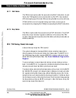
22.4 Pin Name Conventions
The text that follows describes both timers, TIM1 and TIM2. The TIM
input/output (I/O) pin names are T[1,2]CH0 (timer channel 0) and
T[1,2]CH1 (timer channel 1), where “1” is used to indicate TIM1 and “2”
is used to indicate TIM2. The two TIMs share four I/O pins with four
port D I/O port pins. The full names of the TIM I/O pins are listed in
Table 22-1
.
The generic pin names appear in the text that follows.
NOTE:
References to either timer 1 or timer 2 may be made in the following text
by omitting the timer number. For example, TCH0 may refer generically
to T1CH0 and T2CH0, and TCH1 may refer to T1CH1 and T2CH1.
22.5 Functional Description
Figure 22-1
shows the structure of the TIM. The central component of
the TIM is the 16-bit TIM counter that can operate as a free-running
counter or a modulo up-counter. The TIM counter provides the timing
reference for the input capture and output compare functions. The TIM
counter modulo registers, TMODH:TMODL, control the modulo value of
the TIM counter. Software can read the TIM counter value at any time
without affecting the counting sequence.
The two TIM channels (per timer) are programmable independently as
input capture or output compare channels. If a channel is configured as
input capture, then an internal pullup device may be enabled for that
channel.
(See
16.6.3 Port D Input Pullup Enable Register
.)
Table 22-1. Pin Name Conventions
TIM Generic Pin Names:
T[1,2]CH0
T[1,2]CH1
Full TIM
Pin Names:
TIM1
PTD4/T1CH0
PTD5/T1CH1
TIM2
PTD6/T2CH0
PTD7/T2CH1
F
re
e
sc
a
le
S
e
m
ic
o
n
d
u
c
to
r,
I
Freescale Semiconductor, Inc.
For More Information On This Product,
Go to: www.freescale.com
n
c
.
..


