Timer Interface Module (TIM)
Interrupts
MC68HC908GP32
•
MC68HC08GP32
—
Rev. 6
Technical Data
MOTOROLA
Timer Interface Module (TIM)
353
Setting MS0B links channels 0 and 1 and configures them for buffered
PWM operation. The TIM channel 0 registers (TCH0H:TCH0L) initially
control the buffered PWM output. TIM channel 0 status and control
register (TSC0) controls and monitors the PWM signal from the linked
channels.
Clearing the toggle-on-overflow bit, TOVx, inhibits output toggles on TIM
overflows. Subsequent output compares try to force the output to a state
it is already in and have no effect. The result is a 0% duty cycle output.
Setting the channel x maximum duty cycle bit (CHxMAX) and setting the
TOVx bit generates a 100% duty cycle output. (See
22.10.4 TIM
Channel Status and Control Registers
.)
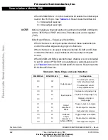
22.6 Interrupts
The following TIM sources can generate interrupt requests:
•
TIM overflow flag (TOF) — The TOF bit is set when the TIM
counter reaches the modulo value programmed in the TIM counter
modulo registers. The TIM overflow interrupt enable bit, TOIE,
enables TIM overflow CPU interrupt requests. TOF and TOIE are
in the TIM status and control register.
•
TIM channel flags (CH1F:CH0F) — The CHxF bit is set when an
input capture or output compare occurs on channel x. Channel x
TIM CPU interrupt requests are controlled by the channel x
interrupt enable bit, CHxIE. Channel x TIM CPU interrupt requests
are enabled when CHxIE = 1. CHxF and CHxIE are in the TIM
channel x status and control register.
22.7 Low-Power Modes
The WAIT and STOP instructions put the MCU in low power-
consumption standby modes.
F
re
e
sc
a
le
S
e
m
ic
o
n
d
u
c
to
r,
I
Freescale Semiconductor, Inc.
For More Information On This Product,
Go to: www.freescale.com
n
c
.
..


