Timer Interface Module (TIM)
I/O Signals
MC68HC908GP32
•
MC68HC08GP32
—
Rev. 6
Technical Data
MOTOROLA
Timer Interface Module (TIM)
355
22.9 I/O Signals
Port D shares four of its pins with the TIM. The four TIM channel I/O pins
are T1CH0, T1CH1, T2CH0, and T2CH1 as described in
22.4 Pin Name
Conventions
.
Each channel I/O pin is programmable independently as an input
capture pin or an output compare pin. T1CH0 and T2CH0 can be
configured as buffered output compare or buffered PWM pins.
22.10 I/O Registers
NOTE:
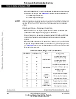
References to either timer 1 or timer 2 may be made in the following text
by omitting the timer number. For example, TSC may generically refer to
both T1SC AND T2SC.
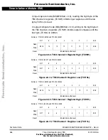
These I/O registers control and monitor operation of the TIM:
•
TIM status and control register (TSC)
•
TIM counter registers (TCNTH:TCNTL)
•
TIM counter modulo registers (TMODH:TMODL)
•
TIM channel status and control registers (TSC0, TSC1)
•
TIM channel registers (TCH0H:TCH0L, TCH1H:TCH1L)
F
re
e
sc
a
le
S
e
m
ic
o
n
d
u
c
to
r,
I
Freescale Semiconductor, Inc.
For More Information On This Product,
Go to: www.freescale.com
n
c
.
..


