Timer Interface Module (TIM)
I/O Registers
MC68HC908GP32
•
MC68HC08GP32
—
Rev. 6
Technical Data
MOTOROLA
Timer Interface Module (TIM)
361
CHxF — Channel x Flag Bit
When channel x is an input capture channel, this read/write bit is set
when an active edge occurs on the channel x pin. When channel x is
an output compare channel, CHxF is set when the value in the TIM
counter registers matches the value in the TIM channel x registers.
When TIM CPU interrupt requests are enabled (CHxIE = 1), clear
CHxF by reading TIM channel x status and control register with CHxF
set and then writing a logic 0 to CHxF. If another interrupt request
occurs before the clearing sequence is complete, then writing logic 0
to CHxF has no effect. Therefore, an interrupt request cannot be lost
due to inadvertent clearing of CHxF.
Reset clears the CHxF bit. Writing a logic 1 to CHxF has no effect.
1 = Input capture or output compare on channel x
0 = No input capture or output compare on channel x
CHxIE — Channel x Interrupt Enable Bit
This read/write bit enables TIM CPU interrupt service requests on
channel x.
Reset clears the CHxIE bit.
1 = Channel x CPU interrupt requests enabled
0 = Channel x CPU interrupt requests disabled
MSxB — Mode Select Bit B
This read/write bit selects buffered output compare/PWM operation.
MSxB exists only in the TIM1 channel 0 and TIM2 channel 0 status
and control registers.
Setting MS0B disables the channel 1 status and control register and
reverts TCH1 to general-purpose I/O.
Reset clears the MSxB bit.
1 = Buffered output compare/PWM operation enabled
0 = Buffered output compare/PWM operation disabled
MSxA — Mode Select Bit A
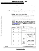
When ELSxB:ELSxA
≠
0:0, this read/write bit selects either input
capture operation or unbuffered output compare/PWM operation.
See
Table 22-3
.
1 = Unbuffered output compare/PWM operation
0 = Input capture operation
F
re
e
sc
a
le
S
e
m
ic
o
n
d
u
c
to
r,
I
Freescale Semiconductor, Inc.
For More Information On This Product,
Go to: www.freescale.com
n
c
.
..


