Memory Map
Input/Output (I/O) Section
MC68HC908GP32
•
MC68HC08GP32
—
Rev. 6
Technical Data
MOTOROLA
Memory Map
49
$0014
SCI Control Register 2
(SCC2)
Read:
SCTIE
TCIE
SCRIE
ILIE
TE
RE
RWU
SBK
Write:
Reset:
0
0
0
0
0
0
0
0
$0015
SCI Control Register 3
(SCC3)
Read:
R8
T8
DMARE
DMATE
ORIE
NEIE
FEIE
PEIE
Write:
Reset:
U
U
0
0
0
0
0
0
$0016
SCI Status Register 1
(SCS1)
Read:
SCTE
TC
SCRF
IDLE
OR
NF
FE
PE
Write:
Reset:
1
1
0
0
0
0
0
0
$0017
SCI Status Register 2
(SCS2)
Read:
BKF
RPF
Write:
Reset:
0
0
0
0
0
0
0
0
$0018
SCI Data Register
(SCDR)
Read:
R7
R6
R5
R4
R3
R2
R1
R0
Write:
T7
T6
T5
T4
T3
T2
T1
T0
Reset:
Unaffected by reset
$0019
SCI Baud Rate Register
(SCBR)
Read:
SCP1
SCP0
R
SCR2
SCR1
SCR0
Write:
Reset:
0
0
0
0
0
0
0
0
$001A
Keyboard Status
and Control Register
(INTKBSCR)
Read:
0
0
0
0
KEYF
0
IMASKK
MODEK
Write:
ACKK
Reset:
0
0
0
0
0
0
0
0
$001B
Keyboard Interrupt Enable
Register
(INTKBIER)
Read:
KBIE7
KBIE6
KBIE5
KBIE4
KBIE3
KBIE2
KBIE1
KBIE0
Write:
Reset:
0
0
0
0
0
0
0
0
$001C
Time Base Module Control
Register
(TBCR)
Read:
TBIF
TBR2
TBR1
TBR0
0
TBIE
TBON
R
Write:
TACK
Reset:
0
0
0
0
0
0
0
0
$001D
IRQ Status and Control
Register
(INTSCR)
Read:
0
0
0
0
IRQF
0
IMASK
MODE
Write:
ACK
Reset:
0
0
0
0
0
0
0
0
Addr.
Register Name
Bit 7
6
5
4
3
2
1
Bit 0
= Unimplemented
R = Reserved
U = Unaffected
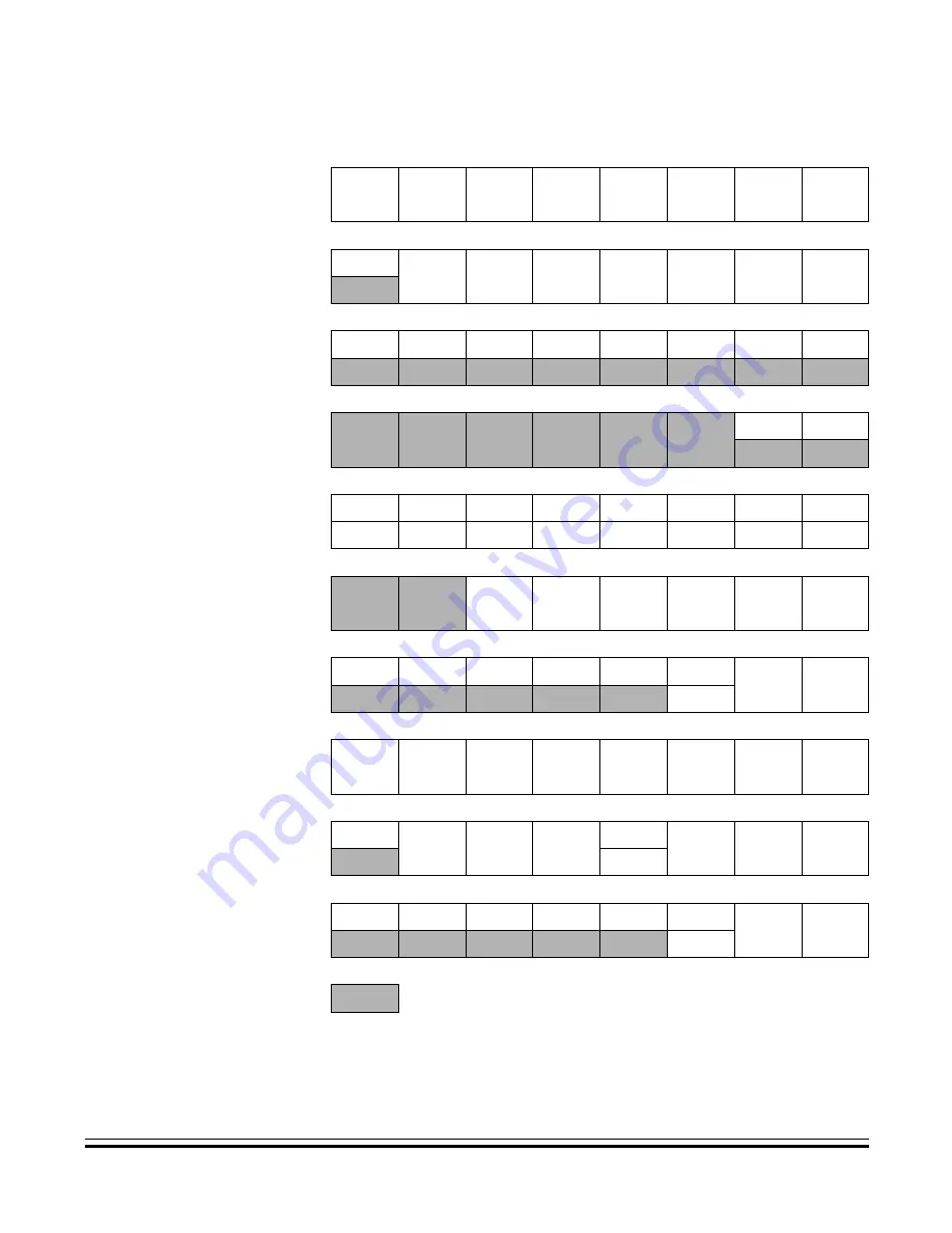
Figure 2-2. Control, Status, and Data Registers (Sheet 3 of 8)
F
re
e
sc
a
le
S
e
m
ic
o
n
d
u
c
to
r,
I
Freescale Semiconductor, Inc.
For More Information On This Product,
Go to: www.freescale.com
n
c
.
..


