Introduction
http://www.motorola.com/computer/literature
5-3
5
Command/response Register Description
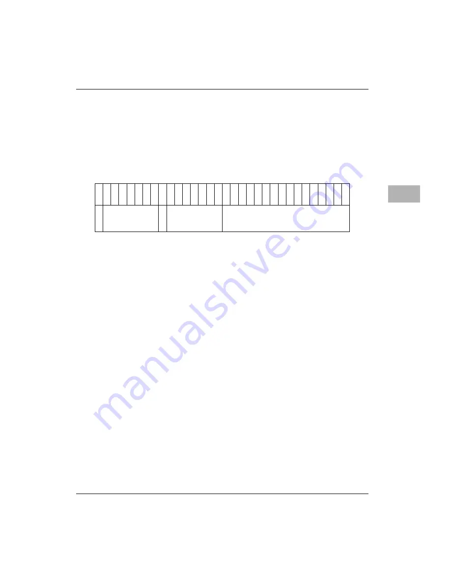
The 2155x SCRATCH7 register is used as the command/response register.
In this register description and the following command descriptions,
references to the upper half of the register refer to bits 0 through 15, and
references to the lower half of the register refer to bits 16 through 31.
Format of command/response register (2155x SCRATCH7):
At reset, hardware clears this register. After reset, firmware writes this
register with the value 0x80525354. This value indicates that a reset event
has occurred and the interface is ready to accept commands.
Bit 0
The ownership flag (OWN). A value of 1 indicates the ‘host’
owns the register. A value of 0 indicates that the local cpu
owns the register.
Bits 1 to 7
7 bit command opcode field. Each command is described in
more detail in the following sections.
Bit 8
Global error status flag (ERR). If the command completed
successfully, then this bit will be written with the value 0 upon
command completion. If the command fails, it will be written
with the value 1. Additional command specific error status
may be returned in other fields of the register.
(register description continues...)
0 1 2 3 4 5 6 7 8 9
1
0
1
1
1
2
1
3
1
4
1
5
1
6
1
7
1
8
1
9
2
0
2
1
2
2
2
3
2
4
2
5
2
6
2
7
2
8
2
9
3
0
3
1
O
W
N
Command opcode
E
R
R
Command Options Command Data/Result
Summary of Contents for MCPN750A
Page 13: ...xii ...
Page 15: ...xiv ...
Page 53: ...1 32 Computer Group Literature Center Web Site Hardware Preparation and Installation 1 ...
Page 67: ...2 14 Computer Group Literature Center Web Site Startup and Operation 2 ...
Page 105: ...5 14 Computer Group Literature Center Web Site Remote Start Via the PCI Bus 5 ...
Page 167: ...7 38 Computer Group Literature Center Web Site Connector Pin Assignments 7 ...
Page 171: ...A 4 Computer Group Literature Center Web Site Specifications A ...
Page 187: ...Index IN 10 Computer Group Literature Center Web Site I N D E X ...


