
2-40
MPC8240 Integrated Processor User’s Manual
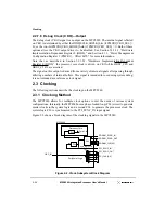
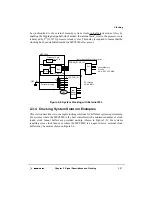
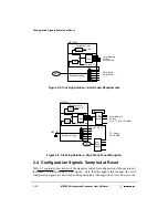
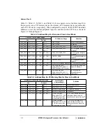
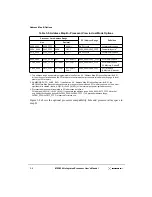
Configuration Signals Sampled at Reset
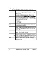
PMAA0
1
Driver capability for the MDH[0:31], MDL[0:31], PAR[0:7], MAA[0:2], and RCS1 signals.
Sets the initial value of the DRV_MEM _CTRL_1 bit in ODCR. Used in combination
with PMAA1, as follows:
1 20-
Ω
data bus drive capability; when this is selected, only 8-
Ω
or 13.3-
Ω
drive
capability allowed for PMAA1
0 40-
Ω
data bus drive capability; when this is selected, only 20-
Ω
or 40-
Ω
drive
capability allowed for PMAA1
PMAA1
1
Driver capability for address signals (RAS/CS[0:7], CAS/DQM[0:7], WE, FOE, RCS0,
SDBA0, SDRAS, SDCAS, CKE, AS, and SDMA[12:0]). Sets the initial value of the
DRV_MEM _CTRL_2 bit in the ODCR register.The meaning of this signal setting
depends on the setting of PMAA0. The two signals and the meaning of their combined
settings for the address signals are shown below:
[PMAA0, PMAA1]:
11 8-
Ω
drive capability
10 13.3-
Ω
drive capability
01 20-
Ω
drive capability
00 40-
Ω
drive capability
PMAA2
1
Driver capability for PCI and EPIC controller output signals. The value of this signal
sets the initial value of ODCR[DRV_PCI].
0 High drive capability on PCI signals (25
Ω
)
1 Medium drive capability on PCI signals (50
Ω
)
QACK
1
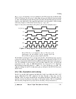
Clock flip disable. When this signal is low on reset, it enables internal clock flipping
logic, which is necessary when the PLL[0:4] signals select a half-clock frequency ratio.
See Section 2.3.3, “Clock Synchronization” for more information on the use of clock
flipping.
0 Clock flip enabled
1 No clock flip
RCS0
1
Boot memory location. The setting of this signal during reset sets the initial RCS0
value in the PICR1 register
0 Indicates that boot ROM is located on the PCI bus.
1 Indicates that boot ROM is located on local processor/memory data bus.
PLL_CFG[0:4]
must
be
driven
These five signals select the clock frequency ratios used by the two PLLs of the
MPC8240. The value of PLL_CFG[0:4] during reset affects the read-only PLLRATIO
field stored in HID1. Note that system software cannot associate the PLLRATIO value
with a unique PLL_CFG[0:4] value.The MPC8240 Hardware Specification lists the
supported settings and provides more detailed information on the clock frequencies.
GNT4
1
Debug address enable. See Section 15.3, “Memory Debug Address”, for more
information about this function.
0 Debug address enabled; partial address of the transaction driven on DA[0:15].
1 Debug address disabled
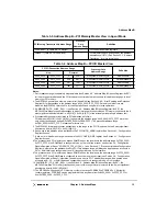
Table 2-5. MPC8240 Reset Configuration Signals (Continued)
Signal Name(s)
Default
State Meaning
Summary of Contents for MPC8240
Page 1: ...MPC8240UM D Rev 1 1 2001 MPC8240 Integrated Processor User s Manual ...
Page 38: ...xviii MPC8240 Integrated Processor User s Manual TABLES Table Number Title Page Number ...
Page 48: ...xlviii MPC8240 Integrated Processor User s Manual Acronyms and Abbreviations ...
Page 312: ...6 94 MPC8240 Integrated Processor User s Manual ROM Flash Interface Operation ...
Page 348: ...7 36 MPC8240 Integrated Processor User s Manual PCI Host and Agent Modes ...
Page 372: ...8 24 MPC8240 Integrated Processor User s Manual DMA Register Descriptions ...
Page 394: ...9 22 MPC8240 Integrated Processor User s Manual I2O Interface ...
Page 412: ...10 18 MPC8240 Integrated Processor User s Manual Programming Guidelines ...
Page 454: ...12 14 MPC8240 Integrated Processor User s Manual Internal Arbitration ...
Page 466: ...13 12 MPC8240 Integrated Processor User s Manual Exception Latencies ...
Page 516: ...16 14 Watchpoint Trigger Applications ...
Page 538: ...B 16 MPC8240 Integrated Processor User s Manual Setting the Endian Mode of Operation ...
Page 546: ...C 8 MPC8240 Integrated Processor User s Manual ...
Page 640: ...INDEX Index 16 MPC8240 Integrated Processor User s Manual ...