4-32
MPC8240 Integrated Processor User’s Manual
Processor Interface Configuration Registers
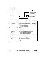
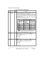
Table 4-27. Bit Settings for PICR2—0xAC
Bits
Name
Reset
Value
Description
31–30
—
00
Reserved
29
NO_SERIAL_CFG
0
This bit controls whether the MPC8240 serializes configuration writes
to PCI devices from the processor.
0 Configuration writes to PCI devices from the processor cause the
MPC8240 to serialize and flush the internal buffers.
1 Configuration writes to PCI devices from the processor do not
cause serialization. The internal buffers are not flushed.
28
—
0
Reserved
27
NO_SNOOP_EN
0
This bit controls whether the MPC8240 generates snoop transactions
on the peripheral logic bus for PCI-to-system memory transactions.
This is provided as a performance enhancement for systems that do
not need to maintain coherency on system memory accesses by PCI.
0 Snooping is enabled.
1 Snooping is disabled.
26
CF_FF0_LOCAL
0
ROM remapping enable. This bit allows the lower 8 Mbytes of the
ROM/Flash address range to be remapped from the PCI bus to the
processor/memory bus. Note that this bit is meaningful only if the
ROM location parameter indicates that ROM is located on PCI bus
(PICR1[RCS0] = 0).
0 ROM/Flash remapping disabled. The lower 8 Mbytes of the
ROM/Flash address space are not remapped. All ROM/Flash
accesses are directed to the PCI bus.
1 ROM/Flash remapping enabled. The lower 8 Mbytes of the
ROM/Flash address space are remapped to the processor/memory
bus. ROM/Flash accesses in the range
0xFF00_0000–0xFF7F_FFFF are directed to the
processor/memory bus. ROM/Flash accesses in the range
0xFF80_0000–0xFFFF_FFFF are directed to the PCI bus.
25
FLASH_WR_LOCKOUT
0
Flash write lockout. This bit, once set, prevents writing to Flash. Once
set, this bit can only be cleared by a hard reset.
0 Write operations to Flash are enabled, provided
FLASH_WR_EN = 1.
1 Write operations to Flash are disabled until the MPC8240 is reset.
24–20
—
0_0000
Reserved
19–18
CF_IP1
11
Internal parameter 1. Should be programmed based on
processor-to-memory clock ratios.
00 Use for all other processor-to-memory clock ratios.
01 Use for 1:1 or 3:2 processor-to-memory clock ratios.
10 Reserved; do not use.
11 Default; however, should be changed to 00 or 01.
17–4
—
All 0s
Reserved
Summary of Contents for MPC8240
Page 1: ...MPC8240UM D Rev 1 1 2001 MPC8240 Integrated Processor User s Manual ...
Page 38: ...xviii MPC8240 Integrated Processor User s Manual TABLES Table Number Title Page Number ...
Page 48: ...xlviii MPC8240 Integrated Processor User s Manual Acronyms and Abbreviations ...
Page 312: ...6 94 MPC8240 Integrated Processor User s Manual ROM Flash Interface Operation ...
Page 348: ...7 36 MPC8240 Integrated Processor User s Manual PCI Host and Agent Modes ...
Page 372: ...8 24 MPC8240 Integrated Processor User s Manual DMA Register Descriptions ...
Page 394: ...9 22 MPC8240 Integrated Processor User s Manual I2O Interface ...
Page 412: ...10 18 MPC8240 Integrated Processor User s Manual Programming Guidelines ...
Page 454: ...12 14 MPC8240 Integrated Processor User s Manual Internal Arbitration ...
Page 466: ...13 12 MPC8240 Integrated Processor User s Manual Exception Latencies ...
Page 516: ...16 14 Watchpoint Trigger Applications ...
Page 538: ...B 16 MPC8240 Integrated Processor User s Manual Setting the Endian Mode of Operation ...
Page 546: ...C 8 MPC8240 Integrated Processor User s Manual ...
Page 640: ...INDEX Index 16 MPC8240 Integrated Processor User s Manual ...


