
4-46
MPC8240 Integrated Processor User’s Manual
Memory Control Configuration Registers
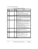
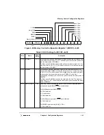
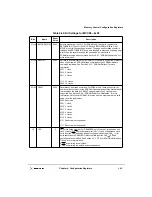
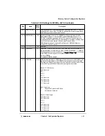
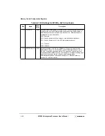
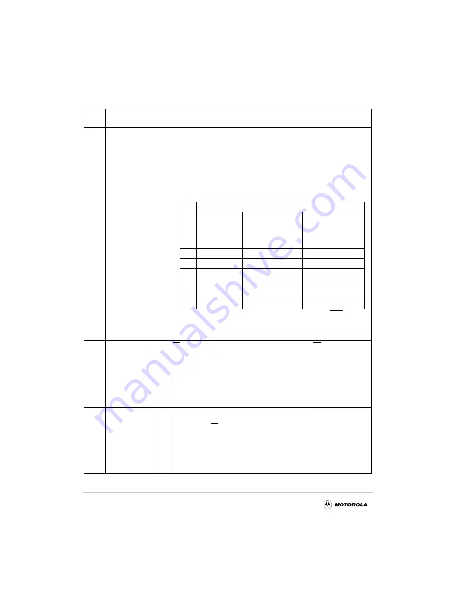
Table 4-39. Bit Settings for MCCR2—0xF4
Bits
Name
Reset
Value
Description
31–29
TS_WAIT_
TIMER[0–2]
000
Transaction start wait states timer. The minimum time allowed for ROM/Flash/Port
X devices to enter high impedance is 2 memory system clocks.
TS_WAIT_TIMER[0–2] adds wait states before the subsequent transaction starts in
order to account for longer disable times of a ROM/Flash/Port X device. This delay
is enforced after all ROM and Flash accesses, delaying the next memory access
from starting (for example, DRAM after ROM access, SDRAM after Flash access,
ROM after Flash access).
Note that this parameter is supported for SDRAM systems only. For EDO/FPM
DRAM systems, TS_WAIT_TIMER[0–2] must = 000.
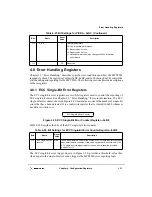
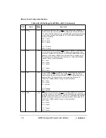
Bits
Wait States for ROM High Impedance
Reads with
wide data path
(32 or 64-bit)
Reads with gather
data path in
flow-through or
registered buffer
mode (8, 16, 32-bit)
All writes
and reads
with gather data path
in in-line buffer mode
(8, 16, 32,-bit)
000
2 clocks
5 clocks
6 clocks
001
2 clocks
5 clocks
6 clocks
010
3 clocks
5 clocks
6 clocks
100
5 clocks
6 clocks
7 clocks
101
6 clocks
7 clocks
8 clocks
111
8 clocks
9 clocks
10 clocks
Note 1. In this context, Flash writes are defined as any write to RCS0 or
RCS1.
Note 2: For Flash writes, add the write recovery time, ROMNAL, to the
given wait states for ROM high-impedance time.
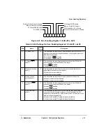
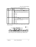
28–25
ASRISE[0–3]
0000
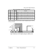
AS rise time. These bits control the rising edge timing of the AS signal for the Port X
interface. See Section 6.4.7, “Port X Interface,” for more information.
0000 Disables AS signal generation
0001 1 clock
0010 2 clocks
0011 3 clocks
...
1111 15 clocks
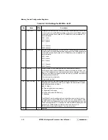
24–21
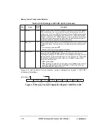
ASFALL[0–3]
0000
AS fall time. These bits control the falling edge timing of the AS signal for the Port X
interface. See Section 6.4.7, “Port X Interface,” for more information.
0000 0 clocks (AS asserted coincident with the chip select)
0001 1 clock
0010 2 clocks
0011 3 clocks
...
1111 15 clocks
Summary of Contents for MPC8240
Page 1: ...MPC8240UM D Rev 1 1 2001 MPC8240 Integrated Processor User s Manual ...
Page 38: ...xviii MPC8240 Integrated Processor User s Manual TABLES Table Number Title Page Number ...
Page 48: ...xlviii MPC8240 Integrated Processor User s Manual Acronyms and Abbreviations ...
Page 312: ...6 94 MPC8240 Integrated Processor User s Manual ROM Flash Interface Operation ...
Page 348: ...7 36 MPC8240 Integrated Processor User s Manual PCI Host and Agent Modes ...
Page 372: ...8 24 MPC8240 Integrated Processor User s Manual DMA Register Descriptions ...
Page 394: ...9 22 MPC8240 Integrated Processor User s Manual I2O Interface ...
Page 412: ...10 18 MPC8240 Integrated Processor User s Manual Programming Guidelines ...
Page 454: ...12 14 MPC8240 Integrated Processor User s Manual Internal Arbitration ...
Page 466: ...13 12 MPC8240 Integrated Processor User s Manual Exception Latencies ...
Page 516: ...16 14 Watchpoint Trigger Applications ...
Page 538: ...B 16 MPC8240 Integrated Processor User s Manual Setting the Endian Mode of Operation ...
Page 546: ...C 8 MPC8240 Integrated Processor User s Manual ...
Page 640: ...INDEX Index 16 MPC8240 Integrated Processor User s Manual ...